If you are considering filing a patent, you should know about the new patent rules effectinve on March 16, 2013. Most importantly, patent rights will switch from “first-to-invent” to “first-to-file.” Before we continue, I am not a lawyer; I’m just a dumb blogger. Seek actual legal advice about the new patent laws if you think… Read More
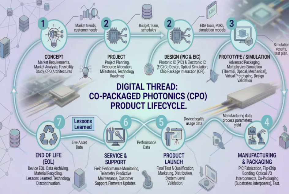 yieldWerx Delivers a Master Class in Co-Packaged Photonics ImplementationWe all know the semiconductor industry is seeing…Read More
 RISC-V Has Momentum. The Real Question Is Who Can DeliverRISC-V has momentum. The industry knows it. The…Read More
 Samtec’s Strong Presence at embedded world 2026The embedded world Exhibition & Conference recently concluded.…Read More
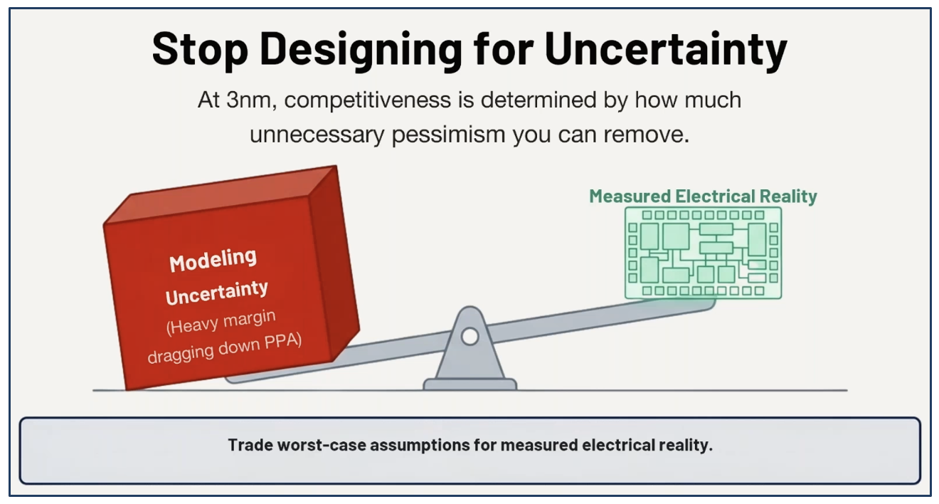 Webinar – How to Reclaim Margin in Advanced NodesThis informative webinar discusses a significant issue that…Read More
Apple and Samsung Do It Again
The numbers are starting to come in for how everyone did in Q4. According to Cannacord Genuity, Apple made 69% of the profit and Samsung made 34%. What do you notice about those numbers? They add up to more than 100%. HTC supposedly made 1% of the profit and everyone else either broke even or lost money. Basically Apple and Samsung have… Read More
Tubes of the Future
So what is a silicon nanowire? It is basically a FET where the active element is a wire 3-20nm in diameter. So where a FinFET has the gate wrapped around 3 sides of the transistor, a nanowire (NW) has it wrapped around all four. In essence, the wire runs through the middle of the gate.
There seem to be three issues about building a silicon… Read More
ARMs in the Clouds
The most interesting session at the Linley Tech Data Center Conference last week was the last one, on Designing Power Efficient Servers. What this was really about was whether ARM would have any success in the server market and what Intel’s response might be.
Datacenters are now very focused on power efficiency and many track… Read More
Notes from Common Platform: Collaborate or Die
FinFETs are hot, carbon nanotubes are cool, and collaboration is the key to continued semiconductor scaling. These were the main messages at the 2013 Common Platform Technology Forum in Santa Clara.
The collaboration message ran through most presenations, like the afternoon talk by Subi Kengeri of GLOBALFOUNDRIES and Joe Sawicki… Read More
No EUV before 7nm?
I was at the Common Platform Technology Forum this week. One of the most interesting sessions is IBM’s Gary Patton giving an overview of the state of semiconductor fabrication. Then, at lunchtime, he is one of the people that the press can question. In this post, I’m going to focus on Extreme Ultra-Violet (EUV) lithography.… Read More
Using Soft IP and Not Getting Burned
The most exciting EDA + Semi IP company that I ever worked at was Silicon Compilers in the 1980’s because it allowed you to start with a concept then implement to physical layout using a library of parameterized IP, the big problem was verifying that all of the IP combinations were in fact correct. Speed forward to today and our… Read More
Semiconductors Down 2.7% in 2012, May Grow 7.5% in 2013
The world semiconductor market in 2012 was $292 billion – down 2.7% from $300 billion in 2011, according to WSTS. The 2012 decline followed a slight gain of 0.4% in 2011. Fourth quarter 2012 was down 0.3% from third quarter. The first quarter of the 2013 will likely show a decline from 4Q 2012 based on typical seasonal patterns and the… Read More
RTL Clock Gating Analysis Cuts Power by 20% in AMD Chip!
Approximately 25% of SemiWiki traffic originates from search engines and the key search terms are telling. Since the beginning of SemiWiki, “low power design” has been one of the top searches. This is understandable since the mobile market has been leading us down the path to fame and fortune. Clearly lowering the… Read More
UVM: Lowering the barrier to IP reuse
One of my acquaintances at Intel must have some of the same viewing habits I do, based on a recent Tweet he sent. He was probably watching “The Men Who Built America” on the History Channel and thinking as I have a lot recently about how the captains of industry managed to drive ideas to monopolies in the late 1800s and early 1900s.
… Read MoreDifference








Intel, Musk, and the Tweet That Launched a 1000 Ships on a Becalmed Sea