Talking about Design IP (I mean successful Design IP) lead you to quickly pronounce the two magic key words: Quality and Ecosystem. Those who remember the IP emergence in the mid 90’s know very well why Quality has to be a prerequisite when dealing with Design IP, as they probably have paid the price of mediocre IP quality at that time.… Read More
 WEBINAR: Reclaiming Clock Margin at 3nm and BelowAt 3nm and below, clock networks have quietly…Read More
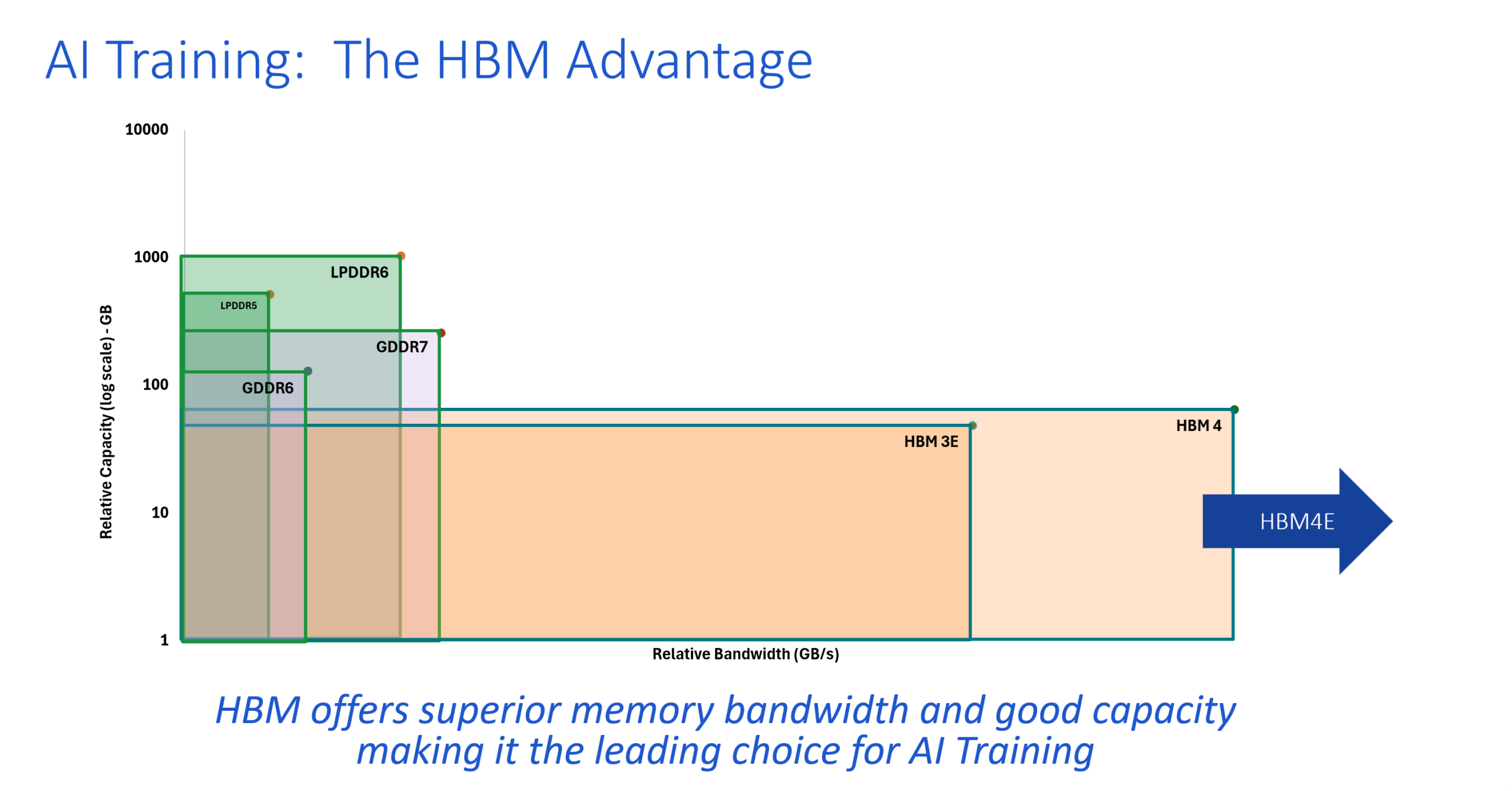
 WEBINAR: HBM4E Advances Bandwidth Performance for AI TrainingThe rapid proliferation of LLMs and other AI…Read More
 Siemens Wins Best in Show Award at Chiplet Summit and Targets Broad 3D IC Design EnablementThe recent Chiplet Summit in Santa Clara was…Read More
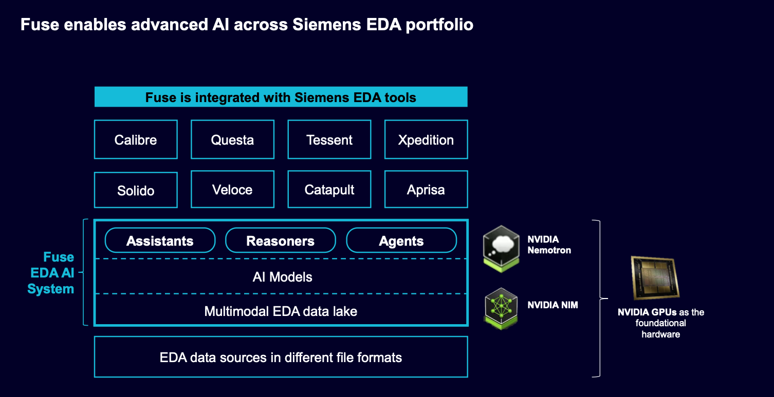
 Siemens Fuse EDA AI Agent Releases to Orchestrate Agentic Semiconductor and PCB DesignThough terminology sometimes get fuzzy, consensus holds that…Read More
Improving Design Practices for an Image Sensor IDM
With nearly twenty five years in business, Tanner EDA Application Engineers have seen a wide range of support requests. One consistent topic area is around design data management and design reuse. In one recent instance, our customer, an IDM who produces imaging sensors for infrared vision systems, called on Tanners AE team for… Read More
How To Design a TSMC 20nm Chip with Cadence Tools
Every process node these days has a new “gotcha” that designers need to be aware of. In some ways this has always been the case but the changes used to be gradual. But now each process node has something discontinuously different. At 20nm the big change is double patterning. At 14/16nm it is FinFET.
Rahul Deokar and John… Read More
Bangers: the Best Beer Bar in Austin; Live Oak Brewing, the Best Beer in Austin
OK, enough with all this semiconductor geeky stuff. The important thing about DAC is…where to go to eat to avoid standard issue convention center chicken Caesar salad.
And a 7 minute walk from the convention center is Bangers Sausage House and Beer Gardenwhere you can have the $8 “executive” lunch consisting… Read More
Wireless Algorithm Validation from System to RTL to Test
This year’s #50DAC will be chock-full of technical content because that is what attracts the masses of semiconductor professionals, like moths to a flame, or like me to a Fry’s Electronics store. Interesting note, I went to high school with Randy Fry. His Dad started the Fry’s supermarket chain which he sold… Read More
The Capital Lite Semiconductor Model
For a couple of years the GSA has had working group looking at funding of semiconductor investment. There is a general feeling, which I share, that it is hard to get a fabless semiconductor company off the ground (nobody would dream of trying to create one with a fab these days) due to the size of the investment and the relatively long… Read More
Cell-Aware Test Seminar
You may have heard about cell-aware testing. It’s a transistor-level test (ATPG) methodology that is quickly becoming a hot topic. If you are involved in DFT and are looking for better quality and reliability, you should definitely know about cell-aware testing.
And lucky you, on May 16, 2013, you can attend a free seminar on cell-aware… Read More
Global Foundries Does DAC
Global Foundries will be at DAC in booth 1314. There will be 6 pods there demonstrating:
- Advanced Technology: 28nm ready and ramping, and next is 20LPM and 14XM.
- PDKs: For 28nm, 20nm and 14nm. 14nm handles FinFET enablement complexity. Robust, easy to use and high quality, supports pretty much the full range of EDA tools.
- Design
A Brief History of Dassault Systèmes
Dassault Systèmes (DS) was created in 1981 when a small team of engineers were spun out of Dassault Aviation. They were developing software to design wind-tunnel models and so reduce the cycle time for wind-tunnel testing, using surface modeling in 3D instead. The company entered into a distribution agreement with IBM that same… Read More
Sage Design Automation iDRM Launch
This is an example of what I do during the day. I work with emerging companies on disruptive technologies and help launch them into the fabless semiconductor ecosystem. This product, iDRM, is the result of three years of joint development work amongst three semiconductor foundries and some of their top customers:… Read More


Chemical Origins of Environmental Modifications to MOR Lithographic Chemistry