You are currently viewing SemiWiki as a guest which gives you limited access to the site. To view blog comments and experience other SemiWiki features you must be a registered member. Registration is fast, simple, and absolutely free so please,
join our community today!
Advanced skill in auto repair, carpentry, plumbing, and similar trades often correlates to one factor. Knowing what you want to do is one thing – having the proper tool is another, and can make the difference. Many a job has extended from minutes to hours over the lack of the right tool at the right moment. Experienced mechanics and… Read More
Semiconductors have played very important role in making internet successful and that has unleashed the potential of e-commerce. Today, we see names like Alibaba, whose primary focus is on commodity trade. I couldn’t imagine an e-commerce type of web portal for semiconductor services until I looked at the eSilicon website. … Read More
Apple reported that it sold $74.6B in products last quarter, and earned an all-time record (for any company) $18.06B in profits. Sammy reported its lowest quarterly profit since 2011 at $21.3Bk, down almost a third.
In 2013 mobile had been 70% of Sammy’s profits so any drop in revenue or profitability would have an amplified… Read More
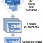
Long Term Evolution (LTE)-based 4G technology is reshaping the wireless infrastructure landscape, and that brings a new set of opportunities for IP core licensor CEVA Inc. and its DSP offerings for multi-mode LTE base stations.
LTE devices—both handsets and radio base stations—are haunted by power constraints, mainly due … Read More
As I have mentioned before, Intel and the foundries approach process development from different starting points. Intel is committed to Moore’s law in reducing the transistor cost by increasing the process density in a near linear fashion. The foundries on the other hand work closely with partners and customers to determine the… Read More
When I hear the phrase Static Timing Analysis (STA) the first EDA tool that comes to mind is PrimeTimefrom Synopsys, and this type of tool is essential to reaching timing closure for digital designs by identifying paths that are limiting chip performance. Sunil Walia, PrimeTime ADV marketing lead spoke with me by phone on Thursday… Read More
What does system on chip (SoC) actually mean? How this tech moniker came into being? There is quite a bit of enigma about SoC in the technology press and what this term really stands for. Roger Shepherd, consultant at Parallel Computer Systems, shares on Quora his version of the SoC story. He says that he first heard about SoCs when … Read More
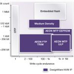
As of today NVM IP has been mostly used in SoC or IC to support very specific needs like analog trimming and calibration or encryption key integration for Digital Right Management (DRM) purpose. In other words small size (less than 1K-bit) few times programmable (FTP) NVM IP was enough to support these needs, thus most of the NVM IP… Read More
Apple’s iPhone 6 alone represents at least 50K wafer starts/month plus the iPad (A8X). What could the Iphone 6S/7 & A9 mean? What about the iWatch? Apple is the technology and volume driver of the semiconductor industry so lets take a look at the broader implications.
If we do the math the A8 is 89mm2 and 8.47 X 10.5mm. Using… Read More
At the end of last year, I moderated a Sonics webinar to introduce the concept of a network-on-chip or NoC. It was called NoC 101 and the replay is still available here.
Well it is a new year and time for chapter 2. I will be moderating a webinar next Wednesday February 4th at 10am pacific time. Once again the webinar itself will be delivered… Read More


Why Huawei Says It Will Match TSMC’s Most Advanced Chips by 2031