Software engineers and firmware designers can find bugs, update their code and re-distribute to the users. In the consumer electronics world this means that my smart phone apps get updated, and my Android OS gets updated on a somewhat regular basis, however on the hardware side the design and verification of an SoC must be close … Read More
 Sensors Converge: Where Intelligence Meets the EdgeThe Sensors Converge Conference is one of the…Read More
 Musk’s Orbital Compute Vision: TERAFAB and the End of the Terrestrial Data CenterAt the TERAFAB launch event in Austin on…Read More
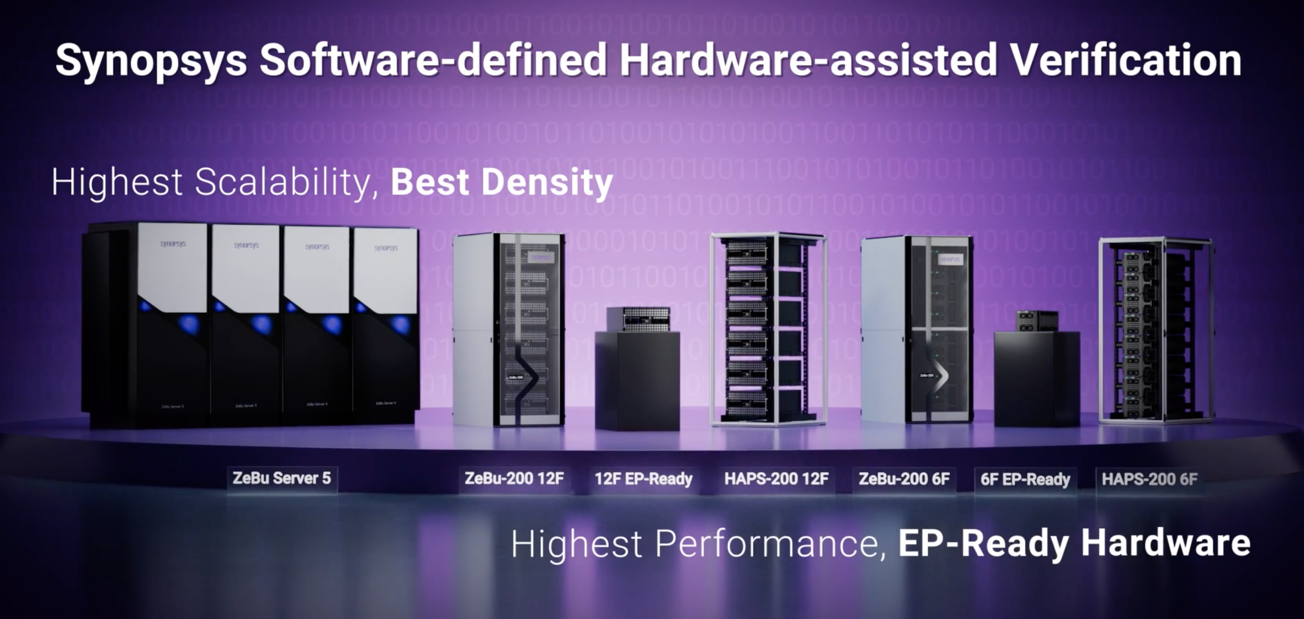
 Synopsys Advances Hardware Assisted Verification for the AI EraAt the 2026 Synopsys Converge Event, Synopsys announced…Read More
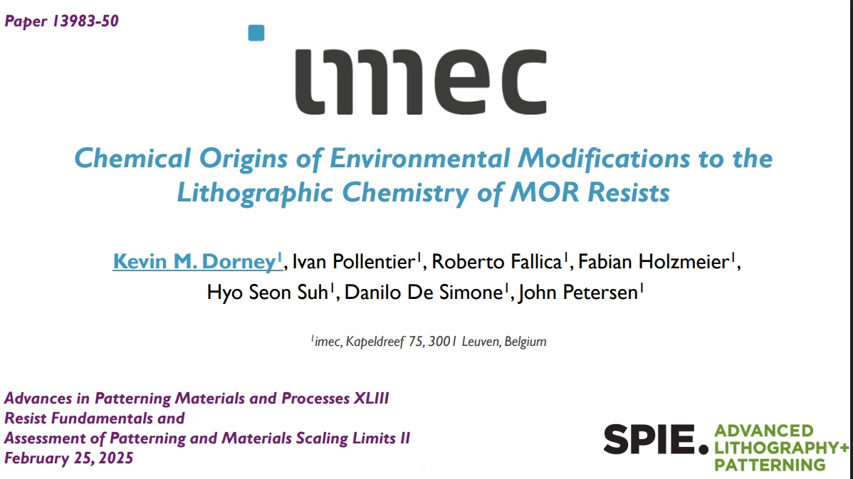
 Chemical Origins of Environmental Modifications to MOR Lithographic ChemistryIn the pursuit of advanced extreme ultraviolet (EUV)…Read More
IDT bolsters RF portfolio amid LTE boom
The global rollout of fourth-generation wireless (4G) infrastructure requires new architectural frameworks for RF devices with demands like high linearity. Integrated Device Technology (IDT) Inc. is confident that its high-performance RF solutions for high-bandwidth communications will open a new window of opportunity… Read More
TSMC Gets Ready for IoT
With all the talk about 14/16nm and 10nm it is important to realize that older processes are still important. Eventually 16nm may end up being cheaper than 28nm but for the time being 28nm seems to be a sort of sweet spot, not just cheaper than every process that came before it (which was true for every new node) but also cheaper than every… Read More
Intel has Another First for 14nm Production!
An interesting thing happened while I was researching a slide from Bill Holt’s “Advancing Moore’s Law” presentation at last month’s analyst meeting. Slide #19 mentioned that Intel was the first to use “air gap” dielectric spaces to improve performance in a digital logic flow for microprocessors. I know a certain foundry that … Read More
CTO Interview with Dr. Wim Schoenmaker of Magwel
I visited the Magwel booth at DAC in June and chatted with Dundar Dumlugol the CEO about their EDA tools that enable 3D co-simulation and extraction. Since then I’ve made contact with their CTO, Dr. Wim Schoenmaker to better understand what it’s like to start up and run an EDA company. Magwel’s history goes back… Read More
Synthesizing rad-tolerant RTL for FPGAs
The maiden voyage of NASA’s Orion spacecraft brought a raft of articles about how the flight computer inside is “no smarter than your phone,” running on wheezing IBM PowerPC 750FX processors. NASA’s deputy manager for Orion avionics, Matt Lemke, admits the configuration is already obsolete – at least in commercial terms. … Read More
What Will Drive Smartphone Market Now?
Whenever a market matures, either it gets plagued by substitutes or it looks for complementary products or technologies which can fuel its maturation curve into further growth opportunities. While PCs and Notebooks got substituted by smartphones, there is no other device in foresight to substitute smartphones. The reason … Read More
A brief history of the Internet of Things
The Internet of Things (IoT) is apparently the next big thing, but it tends to appear in different ways to different people. To some it’s all about connectivity of the web of devices and to other it’s synonymous with sensors and wearable devices. And the scope of IoT is expanding by the day—to smart lighting, smart thermostats, smart… Read More
TSMC Bringing EUV Into Production
Last week was ASML’s investor day. I wasn’t there and they haven’t yet got the material posted on their website, so this is all second hand information. As you know, if you have read any of my comments on EUV, I have been dubious about whether EUV would ever work for production.
The three big problems seem to be:
- source
Xilinx the EDA Company
Like you I cannot believe 2015 is upon us. 15 years ago I remember the Y2K panic. I remember watching the news and noticed the liberal media (they were liberal back then too) just waiting for the first fail somewhere. Ended up like Geraldo at the opening of Al Capone’s Vault. Remember that one? As I persist on with this word salad may I … Read More


Musk’s Orbital Compute Vision: TERAFAB and the End of the Terrestrial Data Center