


For the so-called “2nm” node or beyond, the minimum metal pitch is expected to be 20 nm or even less, while at the same time, contacted gate pitch is being pushed to 40 nm [1]. Therefore, we expect via connections that can possibly be as narrow as 10 nm (Figure 1)! For this reason, it is natural to expect High-NA EUV lithography as the go-to method for patterning at such small scales. However, High-NA’s resolution benefit is offset by its depth of focus [2,3]. A 20 nm defocus can be expected to reduce the width of a spot projected by a High-NA EUV system by 10%. Therefore, the resist cannot be expected to be thicker than 20 nm. This in turn, reduces the density of absorbed photons. A 20 nm thick chemically amplified resist is expected to absorb only 10% of the incident dose. For an incident dose of 60 mJ/cm2, only 4 photons are absorbed per square nanometer! The Poisson statistics of shot noise entails 2sigma of 100%! This will be detrimental for edge roughness (Figure 1). The edge stochastics becomes prohibitive for High-NA EUV.
")
Figure 1. Stochastic EUV photon absorption (6mJ/cm2 averaged over 80 nm x 40 nm). The illumination in the High-NA EUV system is shown on the left.
In fact, even with an 0.33 NA EUV system for 44 nm center-to-center vias or smaller, stochastic edge placement error (EPE) is projected to cause violation of a 5 nm total EPE spec [4]. Therefore, 2nm via patterning is expected to involve serious multipatterning, regardless of whether EUV is used or not.
Figure 2 shows a representative layout for via connections to gates and diffusion areas, where the minimum center-to-center via spacing is 40 nm, and the track pitch is 20 nm. Due to the 40 nm minimum center-to-center spacing constraint, two masks are needed for the gate contacts, while four masks are needed for the source-drain contacts. Note, this number is the same for ArF immersion or EUV. Two vias separated by 40 nm will require two separate masks whether using DUV or EUV.
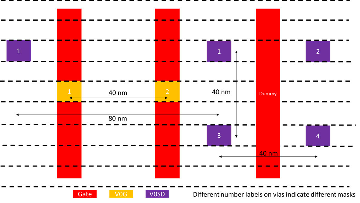
Figure 2. A representative layout for via connections to gate and diffusion areas for contacted gate pitch of 40 nm and track pitch of 20 nm. Different number labels on the vias indicate different masks used for that layer.
For the BEOL, we expect fully self-aligned vias to be used [5]. We can also expect vias to be placed on a crossed diagonal grid [6]. When these arrangements are combined, the number of multipatterning masks can be minimized [7]. Note that multipatterning is still necessary even with EUV as the expected center-to-center distances are still too small (Figure 3). One mask would be needed to overlay a diagonal line grid that blocks half of the crosspoint locations where the two adjacent metal layers overlap (Figure 4). The pitch of this diagonal line grid will require self-aligned quadruple patterning (SAQP) with ArF immersion lithography, and the stochastic defect density cliff below 36 nm pitch [8,9] would also likely force EUV to use self-aligned double patterning (SADP). From the remaining locations, two ArF immersion masks or one EUV mask would be used to select which ones would be kept for forming vias (Figure 5). Note that this would leave a diagonal line signature on the vias (Figure 6).
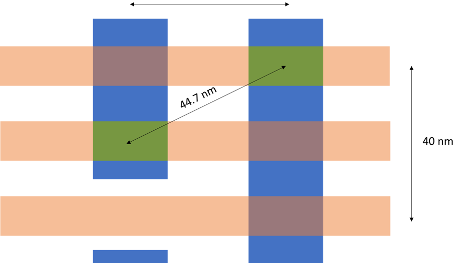
Figure 3. The center-to-center distances above are too small to allow single exposure patterning.
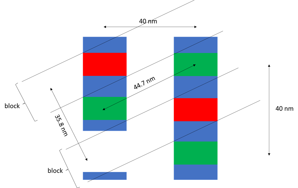
Figure 4. Diagonal line block mask blocks half of the crosspoint locations where the two adjacent metal layers overlap. The blocked overlap locations are in red.
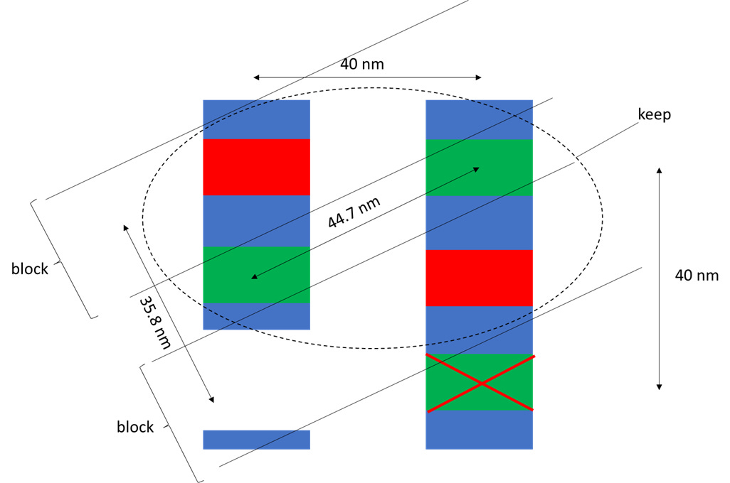
Figure 5. After the diagonal line block grid is in place, a keep mask or masks would select which metal layer locations would be kept for forming vias.
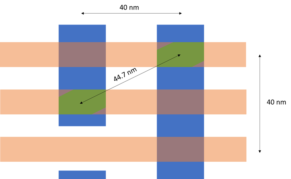
Figure 6. A diagonal line signature is left on the formed vias.
If we note the possible center-to-center distances on the crossed diagonal grid, we can see that relying on the basic repeated litho-etch (LE) approach to multipatterning will lead to up to three masks for EUV, and up to four masks for DUV, making use of an underlying 80 nm x 80 nm pitch tiling (Figure 7). The DUV LE4 approach would definitely be more cost-efficient than EUV LE3 [10]. Hence, any approach to make the requisite multipatterning more efficient, such as the diagonal line grid approach above or even directed self-assembly (DSA) [11], would help ensure getting to 20 nm track pitch and 40 nm contacted gate pitch.
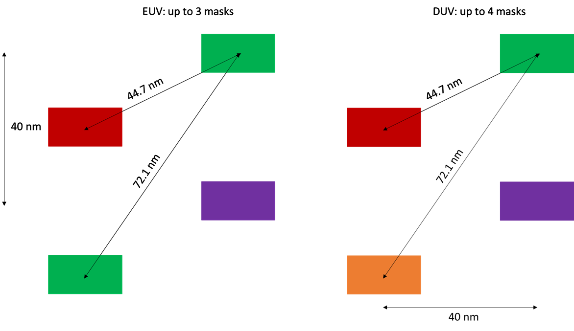
Figure 7. Brute force repeated LE approach could require up to three EUV masks or four DUV masks.
References
[1] I. Cuttress (TechTechPotato), How We Get Down to 0.2nm CPUs and GPUs.
[2] A. Burov, A. V. Pret, R. Gronheid, “Depth of focus in high-NA EUV lithography: a simulation study,” Proc. SPIE 12293, 122930V (2022).
[3] F. Chen, High-NA Hard Sell: EUV Multipatterning Practices Revealed, Depth of Focus Not Mentioned.
[4] W. Gao et al., “Simulation investigation of enabling technologies for EUV single exposure of via patterns in 3nm logic technology,” Proc. SPIE 11323, 113231L (2020).
[5] V. Vashishtha, L. T. Clark, “ASAP5: A predictive PDK for the 5 nm node,” Microel. J. 126, 105481 (2022).
[6] Y-C. Hsiao, W. M. Chan, K-H. Hsieh,US Patent 9530727, assigned to TSMC; S-W. Peng, C-M. Hsiao, C-H. Chang, J-T. Tzeng, US Patent Application US20230387002; F. Chen, Routing and Patterning Simplification with a Diagonal Via Grid.
[7] F. Chen, Multipatterning Reduction with Gridded Cuts and Vias; F. Chen, Exploring Grid-Assisted Multipatterning Scenarios for 10A-14A Nodes.
[8] Y-P. Tsai et al., “Study of EUV stochastic defect on wafer yield,” Proc. SPIE 12954, 1295404 (2024).
[9] Y. Li, Q. Wu, Y. Zhao, “A Simulation Study for Typical Design Rule Patterns and Stochastic Printing Failures in a 5 nm Logic Process with EUV Lithography,” CSTIC 2020.
[10] L-Å. Ragnarsson et al., “The Environmental Impact of CMOS Logic Technologies,” EDTM 2022; E. Vidal-Russell, “Curvilinear masks extend lithography options for advanced node memory roadmaps,” J. Micro/Nanopattern. Mater. Metrol. 23, 041504 (2024).
[11] Z. Wu et al., “Quadruple-hole multiplication by directed self-assembly of block copolymer,” Proc. SPIE 13423, 134231O (2024).


Silicon Insurance: Why eFPGA is Cheaper Than a Respin — and Why It Matters in the Intel 18A Era