Extreme ultraviolet (EUV) lithography targets patterning pitches below 50 nm, which is beyond the resolution of an immersion lithography system without multiple patterning. In the process of exposing smaller pitches, stochastic patterning effects, i.e., random local pattern errors from unwanted resist removal or lack of exposure, have been uncovered due to the smaller effective pixel size and the smaller number of photons absorbed per pixel. In this article, I present a way to visualize the defective pixel rate and how it may be tied to stochastic defect density.
Here, for the most straightforward analysis we will consider an idealized image: a 1:1 duty cycle line grating, with binary amplitude. Also, we will focus on the pitch range of 50 nm and below for a 0.33 NA EUV system. Consequently, the normalized image can be represented mathematically as 0.25+(1/pi)^2+1/pi*cos(2*pi*x/pitch). The absorbed dose profile in the resist will therefore be proportional to this expression, basically multiplied by the absorbed average dose. Again, for keeping things simple, we ignore the polarization and angle-based 3D-mask effects which are actually present, as well as electron blur, which would become much more significant for the 0.55 NA EUV systems [1].
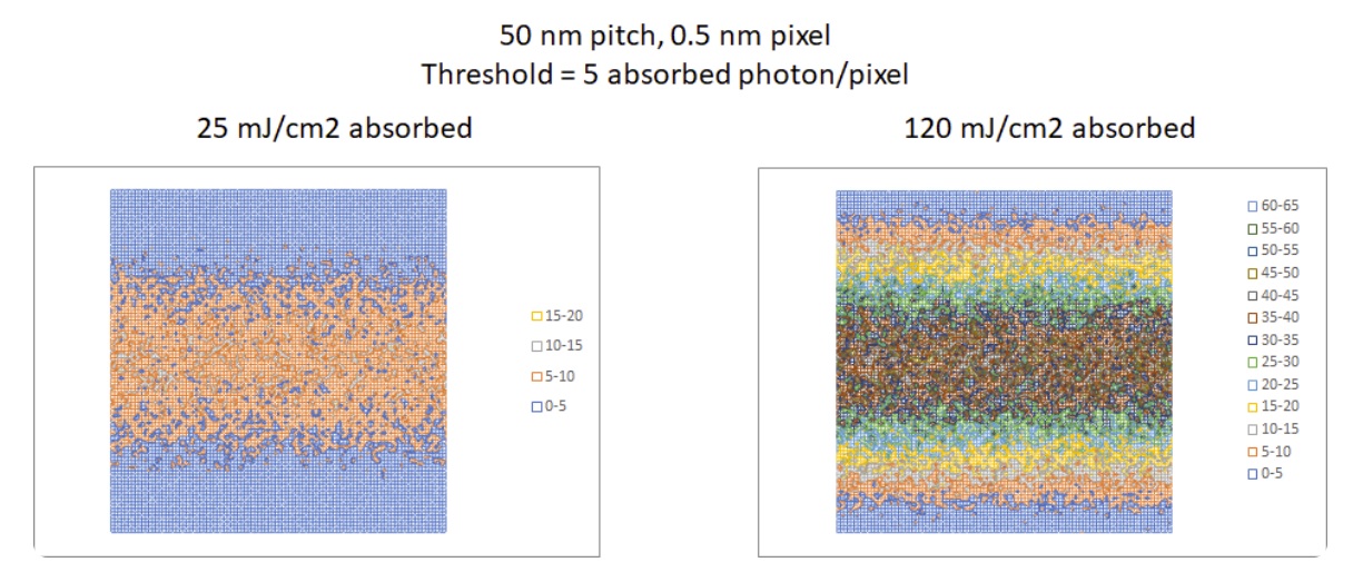
This absorbed dose profile is plotted on a preset grid. I used a 99 x 101 nm pixel grid, where the pixel is normalized to 1/100th of the pitch. Poisson statistics is used to obtain the random absorbed dose at each pixel. The pixel is considered defective if it falls below a certain threshold for exposure, producing an unexposed defect, or if it exceeds the same threshold, producing a potential bridge defect. By changing the dose, improperly unexposed or exposed pixels can be visualized (Figure 1).

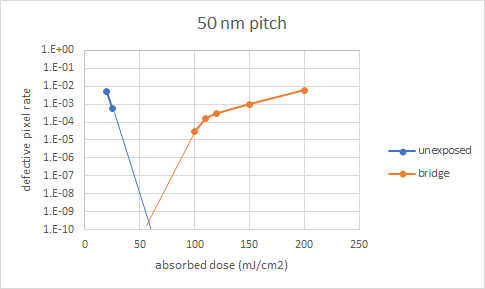
By scanning the dose, the defective pixel rate may be plotted as a function of absorbed dose. Unexposed pixels decrease with increasing dose, while beyond some dose, improperly exposed pixels leading to bridging start increasing (Figures 2,3). The smallest defective pixel rate that can be detected for this small grid is 1e-4. The defective pixel rate is not a direct measure of predicted defect density. Instead, we rely on a formula from de Bisschop [2] used for inspection image pixels: defects/cm2 = 1e14 pixNOK/(NPR), where pixNOK is the defective pixel rate, N is the average number of pixels per defect, P is the pitch, and R is the pixel size in nm. For the 50 nm pitch case, a 3e-10 defective pixel rate with 0.5 nm/pixel and 100 pixels/defect gives 12 defects/cm2. For the 40 nm pitch case, a 1e-9 defective pixel rate with 0.4 nm/pixel and 125 pixels/defect gives 50 defects/cm2. These values are comparable to recently published values [3].


Figure 3. Defective pixel rate (out of 99 x 101 0.4 nm pixels) for 20 nm half-pitch vs. absorbed dose. Optimum absorbed dose and minimum defective rate are higher for the reduced pitch.
At the same average absorbed dose, the smaller pitch shows larger variations due to the smaller pixel size. It is therefore to be expected that larger doses are preferred to maintain a given defective pixel rate. The standard deviation is also smaller for the smaller pitch (due to fewer photons within the grid area), within a given dose range, which would also lead to a higher minimum defect rate.
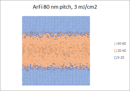
The immensely greater photon density of ArF immersion systems has allowed them to avoid seeing stochastic effects down to the 80 nm pitch (Figure 4), even with relatively low absorbed mJ/cm2.

References
[1] T. Allenet et al., “EUV resist screening update: progress towards High-NA lithography,” Proc. SPIE 12055, 120550F (2022).
[2] P. de Bisschop, “Stochastic printing failures in extreme ultraviolet lithography,” J. Microlith/Nanolith. MEMS MOEMS 17, 041011 (2018).
[3] S. Kang et al., “Massive e-beam metrology and inspection for analysis of EUV stochastic defect,” Proc. SPIE 11611, 1161129 (2021).
This article originally appeared in LinkedIn Pulse: Predicting EUV Stochastic Defect Density
Also Read:
Electron Blur Impact in EUV Resist Films from Interface Reflection
Application-Specific Lithography: 5nm Node Gate Patterning
Spot Pairs for Measurement of Secondary Electron Blur in EUV and E-beam Resists
EUV’s Pupil Fill and Resist Limitations at 3nm
Share this post via:


Musk’s Orbital Compute Vision: TERAFAB and the End of the Terrestrial Data Center