There is growing awareness that EUV lithography is actually an imaging technique that heavily depends on the distribution of secondary electrons in the resist layer [1-5]. The stochastic aspects should be traced not only to the discrete number of photons absorbed but also the electrons that are subsequently released. The electron spread function, in particular, should be quantified as part of resist evaluation [5]. The scale of the electron spread or blur is likely not a well-defined parameter, but itself has some distribution.
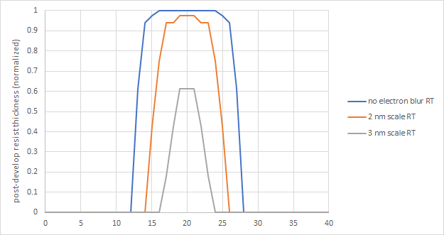
It is necessary to quantitatively assess this distribution of spread. A basic, direct approach is to pattern two features close enough to one another to show resist loss dependent on the electron blur. For example, two 20-25 nm spots separated by a 40 nm center-to-center distance will be significantly affected by 3 nm electron blur scale length, but much less so by 2 nm scale length (see the figure below).

The resist loss between two closely spaced exposed features following development depends on the scale length of the electron spread, a.k.a. blur [5].
An EUV resist or electron-beam resist could be evaluated at a given thickness by evaluating EUV or e-beam exposures of these arrays of these spot pairs in sufficient numbers to get the distribution of electron blur scales, down to the far-out tails, i.e., ppb level or lower. This data would be necessary for better predictions of yield, due to CD variation, edge placement error (EPE), and even the occurrence of stochastic defects.
Interestingly enough, scanning probe electron lithography, such as using an STM, may have the advantage of having probe-to-sample bias limiting the lateral spread of electrons, thereby reducing blur [6]. Again, the spot pair pattern can be used to confirm whether this is true or not.
Reference
[1] J. Torok et al., “Secondary Electrons in EUV Lithography,” J. Photopolymer Sci. and Tech. 26, 625 (2013).
[2] R. Fallica et al., “Experimental estimation of lithographically-relevant secondary electron blur, 2017 EUVL Workshop.
[3] M. I. Jacobs et al., “Low energy electron attenuation lengths in core-shell nanoparticles,” Phys. Chem. Chem. Phys. 19 (2017).
[4] F. Chen, “The Electron Spread Function in EUV Lithography,” https://www.linkedin.com/pulse/electron-spread-function-euv-lithography-frederick-chen
[5] F. Chen, The Importance of Secondary Electron Spread Measurement in EUV Resists,” https://www.youtube.com/watch?v=deB0pxEwwvc
[6] U. Mickan and A. J. J. van Dijsseldonk, US Patent 7463336, assigned to ASML.
This article originally appeared in LinkedIn Pulse: Spot Pairs for Measurement of Secondary Electron Blur in EUV and E-beam Resists
Also Read:
EUV’s Pupil Fill and Resist Limitations at 3nm
ASML- US Seeks to Halt DUV China Sales
Share this post via:


Captain America: Can Elon Musk Save America’s Chip Manufacturing Industry?