As a consequence of having a ~13.5 nm wavelength, EUV photons transfer ~90% of their energy to ionized photoelectrons. Thus, EUV lithography is fundamentally mostly EUV photoelectron lithography. The actual resolution becomes dependent on photoelectron trajectories.
Photoelectron trajectories in EUV lithography were first extensively studied by Kotera et al. [1]. Photoelectrons are preferentially generated along the polarization direction. As EUV light is unpolarized and propagating mostly vertically in the resist, the photoelectron propagation direction tends to be in any random horizontal direction. Thus, the particular direction can be chosen from a uniform random distribution of angles between 0 and 360 degrees. At the same time, the distance traveled can be selected from a random quantile of an exponential distribution [2].
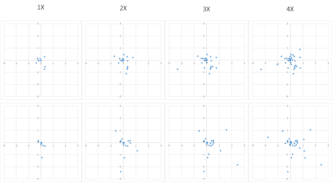
As shown in the figure below, the resulting distribution of distances over which the photoelectrons migrate and deposit their energy is randomly and irregularly shaped. It also depends very much on how many photoelectrons are generated within the same volume of resist, which is proportional to the dose.

EUV photoelectron lateral spread vs. accumulated dose, showing 1X, 2X, 3X, and 4X nominal dose levels. The top and bottom are two separate cases. Initial photoelectron position is (0,0). Nominal 1X dose is 60 mJ/cm2. With an absorption coefficient of 20/um [3], 22% of the light is absorbed in lower half of 40 nm metal-oxide resist, leading to 9 photoelectrons/nm2. Poissonian shot noise is not considered here. Axis labels are in nm.
Increasing the dose very obviously increases the photoelectron spread, effectively increasing the blur. Yet, a higher dose is needed to reduce the impact of Poissonian shot noise, which has not been considered here. The 3-sigma deviation for 9 absorbed photons is 100% [4]! Quadrupling the dose would halve it to 50%. There is therefore an unavoidable resolution-roughness tradeoff in EUV photoresists.
References
[1] M. Kotera et al., “Extreme Ultraviolet Lithography Simulation by Tracing Photoelectron Trajectories in Resist,” Jpn. J. Appl. Phys. 47, 4944 (2008).
[2] https://en.wikipedia.org/wiki/Exponential_distribution
[3] A. Grenville et al., “Integrated Fab Process for Metal Oxide EUV Photoresist,” Proc. SPIE 9425, 94250S (2015).
[4] https://en.wikipedia.org/wiki/Shot_noise
This article first appeared in LinkedIn Pulse: Demonstration of Dose-Driven Photoelectron Spread in EUV Resists


Musk’s Orbital Compute Vision: TERAFAB and the End of the Terrestrial Data Center