EUV lithography systems continue to be the source of much hope for continuing the pace of increasing device density on wafers per Moore’s Law. Recently, although EUV systems were originally supposed to help the industry avoid much multipatterning, it has not turned out to be the case [1,2]. The main surprise has been the rise of stochastic defects and variability [1,2], which challenge both dose and overlay control. It has constrained sub-20 nm features to be printed with multipatterning assistance such as SALELE [3]. This has also accelerated the development of the next-generation High-NA EUV tools [4,5] in order to bring back the opportunity for avoiding multipatterning. On the other hand, High-NA tools have their own concerns as well [4-6].
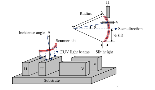
EUV technology requires a substantially different infrastructure from previous optical lithography. A fundamental reason is it is based on reflective optics rather than transmissive optics. Even the mask needs to be built on a reflective multilayer substrate. This, in turn, has led to some distinct quirks in the EUV imaging process. Due to the reflection being an inherently off-axis process, the illumination of the mask has some inherent asymmetry, as shown in Figure 1[7].
Figure 1. EUV illumination of the mask is essentially a rotated off-axis angle across an arc-shaped slit. Illustration is based from Figure 1 in [7].
There is an arc-shaped slit, 26 mm across and ~1-2 mm thick (depending on design), through which a central illumination ray angle of 6 degrees is rotated azimuthally. As a result, features in the center of the exposure field are actually illuminated at different angles from features at the edge of the exposure field. Each different angle produces a different effective “shadow” which comprehends the light’s propagation through and reflection by the multilayer substrate, as well as double pass through the mask pattern [8]. Such shadowing could cause loss of image contrast (also known as fading) [9].
Figure 2. A particular illumination at the slit center is rotated at the slit edge. Illustration is based from Figure 9 in [10].
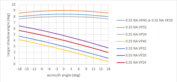
Consequently, the horizontal vs vertical line shadowing behavior varies across slit. The appropriate metric for the degree of shadowing is the larger incident angle, at the mask, in the direction perpendicular to the lines between the two pole angles in an ideal dipole illumination setup (targeting sine=0.5 wavelength/pitch at the wafer) for the slit center. Some results are shown in Figure 3 for horizontal and vertical lines. Low-NA (NA=0.33) and High-NA (NA=0.55) systems are plotted side by side.
Figure 3. Horizontal and vertical line shadowing vs slit position, for different pitches on both 0.33 and 0.55 NA systems.
There are several things to point out.
- In all cases, the smaller pitch has worse shadowing, i.e., a larger incident angle for one of the illumination poles compared to the other.
- The vertical line shadowing varies linearly across slit, because when the azimuthal angle flips sign going from one side of the slit to the other, light is still shining on one side of the line but casts a growing or diminishing shadow.
- The horizontal line shadowing is worse than the vertical line shadowing.
- High-NA tools do not necessarily provide relief from shadowing, particularly for vertical lines, at pitches targeted for High-NA.
- The doubling of demagnification in the High-NA tools from 4x to 8x causes equal shadowing at half the pitch for the latter.
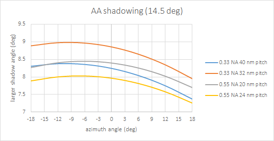
DRAM active areas (Figure 4) present an interesting special case, for they are neither horizontal nor vertical but slanted in between.
Figure 4. Shadowing for DRAM active area lines (angled at 14.5 degrees with respect to the horizontal).
As may be expected, the shadowing for slanted lines has combined characteristics of horizontal and vertical lines. The High-NA tool does not necessarily provide less shadowing than the Low-NA tool, but the range of shadowing across slit is less. Low-NA tools already show significant shadowing for 16-nm half-pitch, while High-NA tools do so for 10-nm half-pitch.
References
[2] D. De Simone and G. Vandenberghe, “Printability study of EUV double patterning for CMOS metal layers,” Proc. SPIE 10957, 109570Q (2019).
[3] K. Sah et al., “Defect characterization of EUV Self-Aligned Litho-Etch Litho-Etch (SALELE) patterning scheme for advanced nodes,” Proc. SPIE 11611, 116112H (2021).
[4] E. van Setten et al., “High NA EUV lithography: Next step in EUV imaging,” Proc. SPIE 10957, 1095709 (2019).
[5] https://www.imec-int.com/en/articles/high-na-euvl-next-major-step-lithography
[6] A. H. Gabor et al., “Effect of high NA “half-field” printing on overlay error,” Proc. SPIE 11609, 1160907 (2021).
[7] P. C. W. Ng et al., “A Fully Model-Based Methodology for Simultaneously Correcting EUV Mask Shadowing and Optical Proximity Effects with Improved Pattern Transfer Fidelity and Process Windows,” Proc. SPIE 7520, 75200S (2009).
[8] E. van Setten et al., “Multilayer optimization for high-NA EUV mask3D suppression,” Proc. SPIE 11517, 115170Y (2020).
[9] C. van Lare, F. Timmermans, and J. Finders, “Mask-absorber optimization: the next phase,” J. Micro/Nanolith. MEMS MOEMS 19, 024401 (2020).
[10] H. Tanabe, “Classification of EUV masks based on the ratio of the complex refractive index k/(1-n),” Proc. SPIE 11854, 11581416 (2021).
This article originally appeared in LinkedIn Pulse: Horizontal, Vertical , and Slanted Line Shadowing Across Slit in Low-NA and High-NA EUV Lithography Systems


Captain America: Can Elon Musk Save America’s Chip Manufacturing Industry?