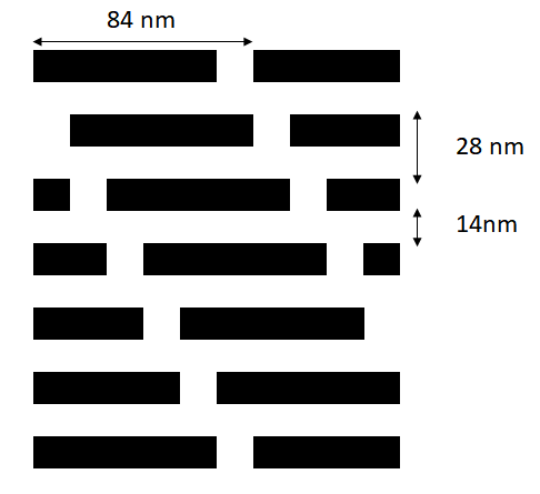
In the recent DRAM jargon, “1X”, “1Y”, “1Z”, etc. have been used to express all the sub-20 nm process generations. It is almost possible now to match them to real numbers which are roughly the half-pitch of the DRAM active area, such as 1X=18, 1Y ~ 17, etc. At this rate, 14 nm is somewhere around “1B”, and is some time away, maybe 2021 at earliest. Still, it is a good exercise to ponder the patterning possibilities of a 14 nm DRAM, using the representative pattern shown in Figure 1. Note that the layout is 6F2, which leaves too little distance between the transistor gates (9F2 would be more realistic [1]).
Figure 1. 14 nm half-pitch DRAM active area.
This pattern has some noteworthy symmetries. It repeats every six rows. Each row is also shifted by a sixth of a pitch. This greatly simplifies the diffraction pattern spectrum, consisting of plane waves exp[i*(m*2*pi*x/xpitch + n*2*pi*y/ypitch)], where m and n cover all integers. Only when m and n add up to a multiple of 6 will the plane waves be non-vanishing (see Appendix for proof).
Single EUV exposure
Of course, with the availability of EUV tools, single exposure using EUV is the first considered option. The possible diffraction patterns from Figure 1 for all the points in the pupil are shown in Figure 2.
Figure 2. Diffraction patterns for the pattern of Figure 1, originating from all possible different directions of illumination [2].
The radial distance here represents the sine of the illumination angle (multiplied by the system magnification of 4). The largest distance corresponds to the numerical aperture (NA) of 0.33, which is the upper limit for any angle. The points with radial distance up to 30% NA cannot resolve the individual horizontal rows, while the remaining pupil area includes altogether ~30 diffraction patterns, each taking its share of the photon dose. Assuming a 30 mJ/cm2 dose gives an average of ~1 mJ/cm2 per diffraction pattern. This gives less than one photon per square nanometer for each diffraction pattern, a very noisy image indeed! An average of ~3% pupil fill per diffraction pattern makes pupil fill a concern for throughput [3] unless several patterns are included, forcing us to walk back this only way to address the photon division problem.
EUV 28 nm pitch lines
It’s quite straightforward to find an optimum EUV source pattern for 28 nm pitch, which requires only two diffraction orders (0th and 1st). Figure 3 shows all the points which give at most 30 degrees phase shift between the 0th and 1st orders at 30 nm defocus.
Figure 3. Optimized dipole source for 28 nm pitch (13.5 nm wavelength, 0.33 NA).
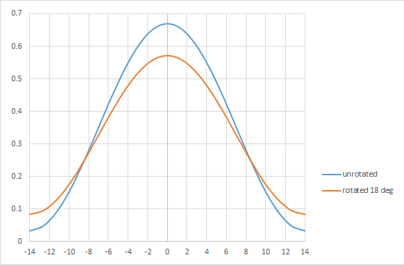
However, due to rotation across the field [4], a rotation of 18 degrees already misplaces more than 20% of the source points, leading to a noticeable change in the image (Figure 4).
Figure 4. Dipole rotation effect across field significantly affects the 28 nm pitch image.
SAQP with cuts
Due to the fundamental issues of using EUV for the 28 nm pitch active area pattern shown above, self-aligned quadruple pattern (SAQP) starting with immersion lithography would have to be used. Since the SAQP is to produce regular lines in an array, the process flow is straightforward but care must always be taken to suppress or minimize pitch walking [5].
The cuts for the lines may be trickier, although they offer tighter line end gaps. Perhaps a single diagonal cut line (which can be done by immersion lithography) across all rows is tolerable without shaving too much of the line ends of the active area. Otherwise, a self-aligned cut process in DUV is preferred to EUV, due to overlay and stochastic concerns [5-7].
Summary of approaches
The 28 nm pitch DRAM active area patterning approaches covered above are summarized below:
Appendix: Vanishing diffraction orders in staggered arrays
A periodic function f(x) can be represented as a Fourier series, with x normalized to pitch:
In two dimensions, we can proceed similarly, normalizing both x and y with respect to x-pitch and y-pitch, respectively:
Each coefficient cmn is obtained through an integral:
For the staggered array of Figure 1, f(x) can be defined for different ranges of y, within the y-pitch, as follows:
f(x,y) = 1, 0<x<1/6, 0<y<1/6, (sub-pitch row 0)
1/6<x<2/6, 1/6<y<2/6, (sub-pitch row 1)
2/6<x<3/6, 2/6<y<3/6, (sub-pitch row 2)
3/6<x<4/6, 3/6<y<4/6, (sub-pitch row 3)
4/6<x<5/6, 4/6<y<5/6, (sub-pitch row 4)
5/6<x<1, 5/6<y<1 (sub-pitch row 5)
0, elsewhere
The integral for cmn for the jth row has the similar expression:
which is equal to sin(pi*m/6)/(pi*m)*sin(pi*n/6)/(pi*n)*exp[-ipi*m/6]exp[-ipi*n/6] exp[-i2pi*j(m+n)]/6]. For the special case m equal to 0, the sin(pi*m/6)/(pi*m) is replaced by 1/6.
Since this is for the jth row, the final value of cmn requires a sum from j=0 to j=5. When m+n is an integral multiple of 6, exp[-i2pi*j(m+n)]/6] = 1, so the sum adds up to 6, but when m+n is an integer that is not a multiple of 6, the sum in fact adds up to 0. This is because in this case 2pi(m+n)/6 represents a rotation going 1/6, 2/6, 3/6, … of the way around a circle, and adding 6 such consecutive rotations always gets you back to where you started; zero distance is traveled. The picture is consistent with the previous case with exp[-i2pi*j(m+n)]/6] = 1 as it can be understood as adding 6 unit vectors in a row, so the final distance traveled is 6.
So, for the staggered array of Figure 1, we see that cmn is 0 unless m+n is a multiple of 6.
References
[1] K. Lee, D. Kim, C. Yoon, T. Park, S. Han, Y. Hwang, K. Lee, H. Kang, H. Kim, “Self-aligned double patterning for active trim contacts with anisotropic pattern pitches in sub-20 nm dynamic random access memories,” J. Microlith/Nanolith. MEMS MOEMS 18, 040501 (2019).
[2] https://www.linkedin.com/pulse/need-low-pupil-fill-euv-lithography-frederick-chen
[3] M. van de Kerkhof, H. Jasper, L. Levasier, R. Peeters, R. van Es, J-W. Bosker, A. Zdravkov, E. Lenderink, F. Evangelista, P. Broman, B. Bilski, T. Last, “Enabling sub-10nm node lithography: presenting the NXE:3400B EUV scanner,” Proc. SPIE 10143, 101430D (2017).
[4] S-S. Yu, A. Yen, S-H. Chang, C-T. Shih, Y-C. Lu, J. Hu, T. Wu, “On the Extensibility of Extreme-UV Lithography,” Proc. SPIE 7969, 79693A (2011).
[5] https://www.linkedin.com/pulse/application-specific-lithography-5nm-6-track-cell-frederick-chen
[6] U. S. Patent 10,115,726, assigned to Tokyo Electron Ltd.
[7] A. Raley, N. Mohanty, X. Sun, R. A. Farrell, J. T. Smith, A. Ko, A. W. Metz, P. Biolsi, A. Devilliers, “Self-Aligned Blocking Integration Demonstration for Critical sub 40nm pitch Mx Level Patterning,” Proc. SPIE 10149, 101490O (2017).


Musk’s Orbital Compute Vision: TERAFAB and the End of the Terrestrial Data Center