The traditional ways of boosting computing throughput are either to increase operating frequency or to use multiprocessing. The industry has done a good job of applying these techniques to maintain a steady increase in performance. However, there is a discontinuity in the needs for processing power. Artificial Intelligence (AI) is creating an exponential increase in throughput. Strategies for delivering more performance for AI have included moving to increased numbers of processors and moving to architectures that include GPUs and FPGAs.
Nonetheless, hard obstacles exist in using these approaches. For starters, processor speeds have been frozen at ~4GHZ for quite some time. This is why parallel processing has become the method of choice. Yet, as the number of processing elements increase, the performance per processor decreases as overhead ramps up. This is a result of a combination of hardware limitations and the difficulty in fully utilizing in software the available computing power. With multiprocessing, GPUs or FPGAs, there is consistently a bottleneck with the ‘head end’ processor. AI exacerbates this with its inherently parallel operation with massive peer-to-peer data transfer needs.
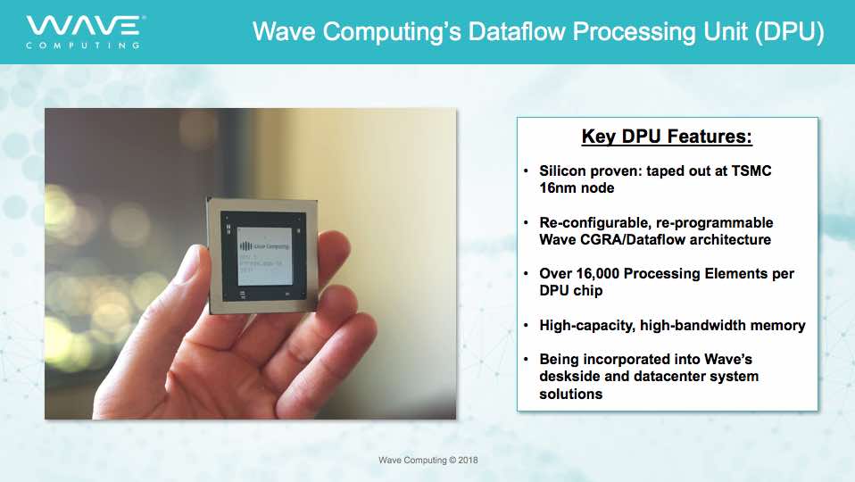
Wave Computing has developed systems that use a completely new, underlying dataflow processor architecture optimized to run machine learning (ML) workloads effortlessly and at scale. Their massively parallel data processor unit (DPU) chips contain 16,000 individual processors that are highly interconnected. Each processor runs non-branching instruction sequences, handling training or inference tasks at clock rates pushing 6 GHz. This is possible because they have eschewed a global clock signal and use an elegant synchronization method to keep the processors in step with each other.

In the Wave Compute Appliance, multiple chips are used to achieve up to 128,000 processing elements per appliance. Four appliances can be combined to provide 512,000 processing elements.
The hard work of delegating processing across the reconfigurable array is done up front with their programming tools. Without the need for a central task scheduler, their solution avoids a major potential choke point. In addition to a throughput advantage, their approach offers a significant energy advantage with the deskside system consuming no more than 0.16kW.
Naturally, the system connectivity and memory needs to be optimized to take advantage of their dataflow architecture. Their DPU boards have slots for 32GB of interconnected high-speed, high-bandwidth DRAM, and are equipped with 512GB of DDR4 high-capacity DRAM. Additionally, there is PCIe connectivity. Wave Computing had the task of building in extensive and varied high-speed off chip interfaces. To meet their power and performance needs at 16nm, they tapped Analog Bits for the SOC’s critical SerDes IP.
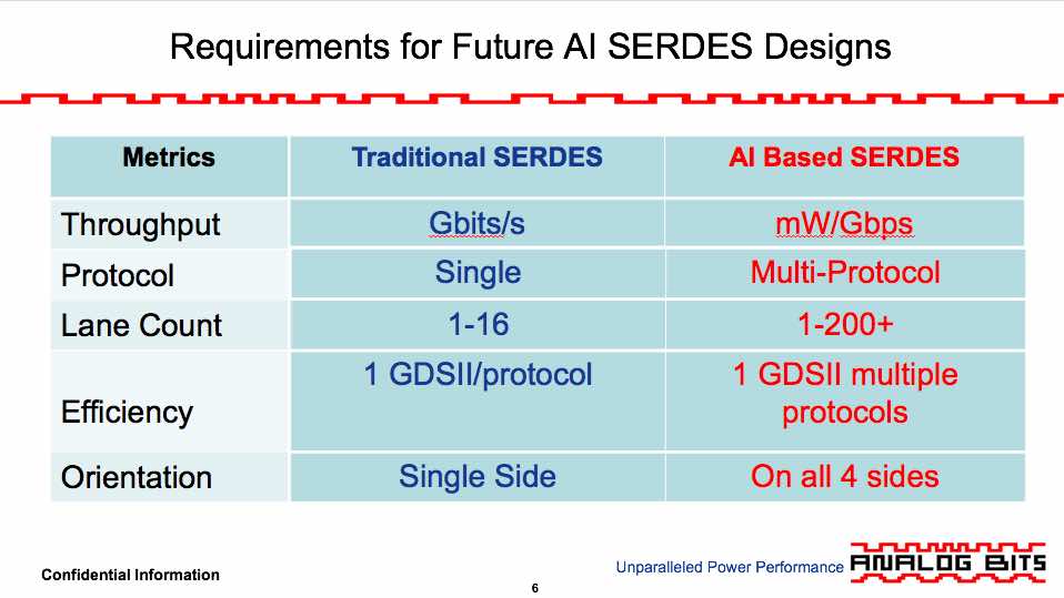
Using optimized SerDes can save a lot of area and power, given the increasing portion of a total chip’s resources they are consuming in newer designs, with many lanes and higher data rates. Wave Computing wanted to provision SerDes that matched the power sipping characteristics of their DPUs. Analog Bits offers a state-of-the-art, non-LC based SerDes that supports multiple protocols and is tolerant of metallization and orientation changes. This means that on three sides of their DPU, Wave Computing was able to use the one SerDes to support all their needs. Analog Bits’ 16nm low-power SerDes needs only 4mW/Gbps to operate up to 10Gbps. Above 16Gbps, their solution only uses 6.5mW/Gbps.

Wave Computing estimates that AI training can use 80% of data center capacity. Deploying a faster and more energy efficient data center resource for this activity could dramatically change AI performance and its carbon footprint. A side benefit will be the ability to allow for more experimentation and ultimately the development of better algorithms. A data scientist could have a supercomputer at their deskside for their dedicated use. Alternatively, with lower power densities and more compact packaging, serious computing power can move from the cloud closer to the edge to provide lower latency and better data fusion.
Comprehensive information about Analog Bits’ analog IP can be found on their website. To learn more about Wave Computing’s solution that uses this IP, I suggest looking on their website and checking out the white papers on their dataflow technology.
About Wave: Wave Computing is revolutionizing the deep learning industry by enabling organizations to drive better business value from their data with its roadmap of WaveFlow™ computing systems. The company’s innovative system solutions based upon dataflow technology provide high-performance training and high-efficiency inferencing at scale, bringing deep learning to customers’ data wherever it may be. Wave Computing was named a Machine Learning Industry Technology Innovation Leader by Frost & Sullivan, and a Top 25 Artificial Intelligence Provider by CIO Application Magazine.
About Analog Bits:Founded in 1995, Analog Bits, Inc. (www.analogbits.com), is a leading supplier of mixed-signal IP with a reputation for easy and reliable integration into advanced SOCs. Products include precision clocking macros such as PLLs & DLLs, programmable interconnect solutions such as multi-protocol SERDES and programmable I/O’s as well as specialized memories such as high-speed SRAMs and TCAMs. With billions of IP cores fabricated in customer silicon and design kits supporting processes from 0.35-micron to 7nm, Analog Bits has an outstanding heritage of “first-time-working” with foundries and IDMs.
Also Read:
7nm SERDES Design and Qualification Challenges!
CEO Interview: Alan Rogers of Analog Bits
IP development strategy and hockey
Share this post via:


Comments
One Reply to “AI processing requirements reveal weaknesses in current methods”
You must register or log in to view/post comments.