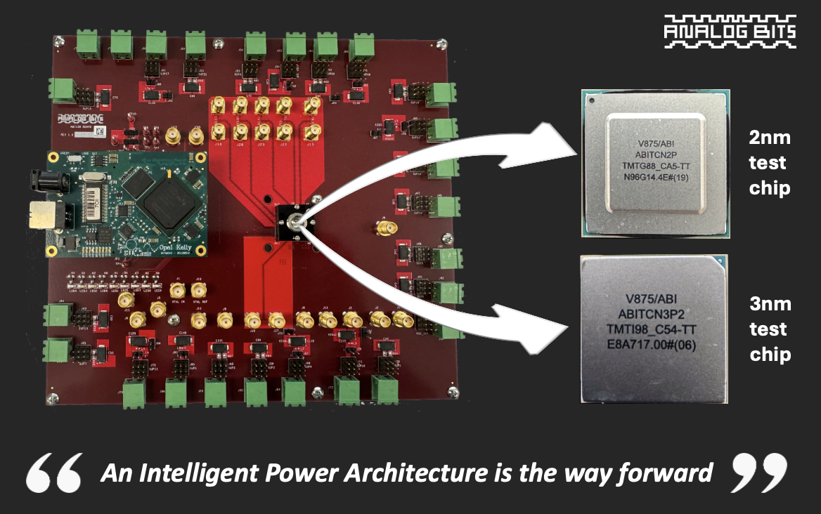
The TSMC Technology Symposium recently kicked off in Santa Clara, with a series of events scheduled around the world. This event showcases the latest TSMC technology. It is also an opportunity for TSMC’s vast ecosystem to demonstrate commercial application on TSMC’s technology. There is a lot to unpack at an event like this. There are great presentations and demonstrations everywhere, but occasionally a company rises above the noise and grabs the spotlight with unique or memorable news.
My view is that Analog Bits stepped into the spotlight this year with cutting-edge analog IP on the latest nodes and a strategy that will change the way design is done. Let’s examine how Analog Bits steals the show with working IP on TSMC 3nm and 2nm and a new design strategy.
Blazing the Trail to 2nm
Working silicon demonstrations of TSMC’s CLN2P technology represent rare air at this TSMC event. Analog Bits recently completed a successful second test chip tapeout at 2nm, but the real news is the company also came to the show with multiple working analog IPs at 2nm. Six precision IPs were demonstrated, the locations of those blocks on the test chip is shown below and the finished chip pictured at the top of this post.
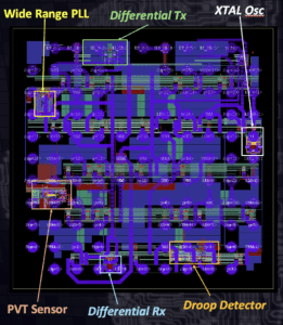
What follows are some details from the cutting edge. Let’s begin with the wide range PLL. Features of this IP include:
- Electrically programmable for multiple applications
- Wide range of input and output frequencies for diverse clocking needs
- Implemented with Analog Bits’ proprietary architecture
- Low power consumption
- Spread spectrum tracking capability
- Requires no additional on-chip components or bandgaps, minimizing power consumption
- Excellent jitter performance with optimized noise rejection
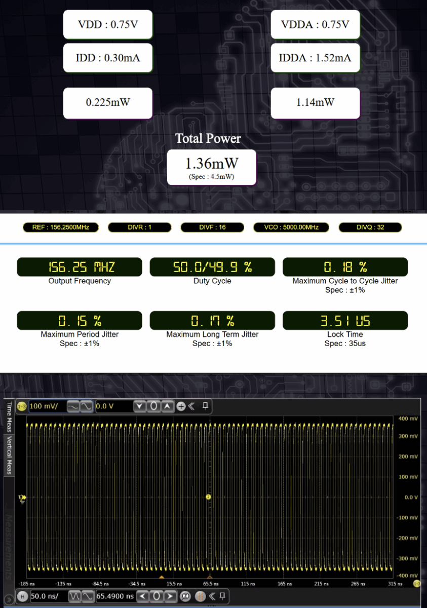
The figure below illustrates some power and jitter numbers. Note the jitter data is for the whole test setup, test chip output buffers, test board, measurement equipment, and not a de-embedded number of the PLL standalone.
Next is the PVT sensor. IPs like this are critical for managing power and heat. There will be more on power management in a bit. Features of this IP include:
- High accuracy thermometer is a highly integrated macro for monitoring temperature variation on-chip
- Industry leading accuracy untrimmed, with easy trimming procedures
- An additional voltage sample mode is included allowing for voltage monitoring
- The block includes a simple-to-use digital interface that works with standard core and IO level power supplies
- Implemented with Analog Bits’ proprietary architecture
- Low power consumption
Demonstrations included showcasing the temperature accuracy and temperature and voltage linearity of the IP.
Next is a droop detector. Voltage droop is another key item for power management. It occurs when the current in the power delivery network (PDN) abruptly changes, often due to workload fluctuations. This effect can lead to supply voltage drops across the chip which can cause performance degradation, reduce energy efficiency, and even result in catastrophic timing failures. Feature of this IP include:
- Integrated voltage reference for stand-alone operation
- Easy to integrate with no additional components or special power requirements
- Easy to use and configure
- Programmable droop detection levels
- Low power
- Implemented with Analog Bits’ proprietary architecture
- Requires no additional on-chip macros, minimizing power consumption
The next IP is an 18-40MHz crystal oscillator. Features for this IP include:
- Pad macro that supports most industry standard crystals in the 18-40MHz range
- Uses standard CMOS transistors
- Power-down option for IDDQ testing
- Oscillator by-pass mode option for logic testing
- Self-contained ESD protection structure
And finally, the differential transmit (TX) and receive (RX) IP blocks. Features here include:
TX
- Wide frequency range support up to 2,000 MHz output for diverse clocking needs
- Implemented with Analog Bits’ proprietary architecture
- Low power consumption
- Requires no additional on-chip components or bandgaps, minimizing power consumption
RX
- Differential clock receiver
- Single-ended output to chip core
- Wide ranges of input frequencies for diverse clocking needs
- Implemented with Analog Bits’ proprietary architecture
- Low power consumption
- Programmable termination
- Spread spectrum tracking capability
- Requires no additional on-chip components or bandgaps, minimizing power consumption
On the Cutting Edge with 3nm IP
Four power management IPs from TSMC’s CLN3P process were also demonstrated at the show. The test chip these IPs came from is also pictured in the graphic at the top of this post. The IPs demonstrated include:
A scalable low-dropout (LDO) regulator. Features of this IP include:
- Integrated voltage reference for precision stand-alone operation
- Easy to integrate with no additional components or special power requirements
- Easy to use and configure
- Scalable for multiple output currents
- Programmable output level
- Trimmable
- Implemented with Analog Bits’ proprietary architecture
- Requires no additional on-chip macros, minimizing power consumption
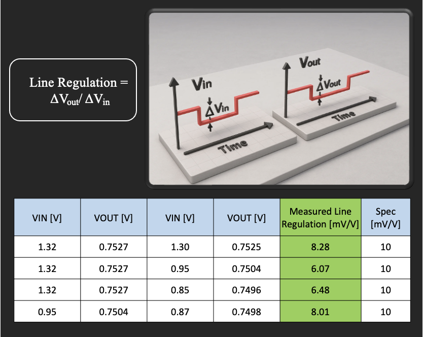
The line regulation performance of this IP is shown in the figure below.
Next is a spread spectrum clock generation PLL supporting PCIe Gen4 and Gen5. Features of this IP include:
- High performance design emphasis for meeting low jitter requirements in PCIe Gen4 and Gen5 applications
- Implemented with Analog Bits’ proprietary LC architecture
- Low power consumption
- Spread spectrum clock generation (SSCG) and tracking capability
- Excellent jitter performance with optimized noise rejection
- Calibration code and bandgap voltage observability (for test)
- Requires no additional on-chip components, minimizing power consumption
A high-accuracy thermometer IP using Analog Bits patented pinless technology was also demonstrated. Features of this IP include:
- IP is a highly integrated macro for monitoring temperature variation on-chip
- Industry leading accuracy untrimmed, with easy trimming procedures
- An additional voltage sample mode is included allowing for voltage monitoring
- The block includes a simple-to-use digital interface that works with just standard core and power supply saving customers analog routing and simplifying package design
- Pinless technology means the IP is powered by the core voltage, no analog power pin is required
- Low power consumption
Voltage linearity for this IP is shown in the figure below.
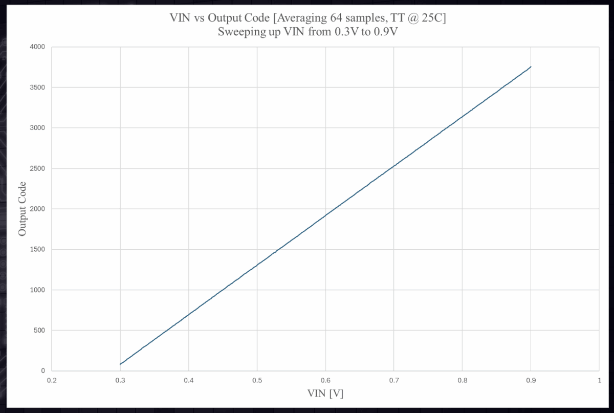
And finally, a droop detector for 3nm. Features include:
- Integrated voltage reference for stand-alone operation
- Easy to integrate with no additional components or special power requirements
- Easy to use and configure
- Programmable droop detection levels
- Low power
- Implemented with Analog Bits’ proprietary architecture
- Requires no additional on-chip macros, minimizing power consumption
Intelligent Power Architecture Launches a New Design Strategy
Innovation brings new challenges. A big design challenge is optimizing performance and power in an on-chip environment that is constantly changing, is prone to on-chip variation and is faced with all kinds of power-induced glitches. As multi-die design grows, these problems are compounded across many chiplets that now also need a high-bandwidth, space-efficient, and power-efficient way to communicate.
This problem cannot be solved as an afterthought. Plugging in optimized IP or modifying software late in the design process will not be enough. Analog Bits believes that developing a holistic approach to power management during the architectural phase of the project is the only path forward.
It is against this backdrop that the company announced its Intelligent Power Architecture initiative at the TSMC Technology Symposium. The company stated that its high-accuracy on-die PVT sensors, process performance monitors, integrated power-on resets, droop detectors, LDOs, and glitch catchers all work together with its low power SerDes, ADCs and pinless IP libraries to deliver a power management architecture that will meet the most demanding requirements. Pinless IP technology, invented by Analog Bits, will become even more critical to migrate below 3nm as all of the IP will work directly from the core voltage. The technology is already proven in production silicon on N5 and N3.
Analog Bits stated the company is already working with large, successful organizations that are building some of the most power-hungry chips in the world to achieve this goal. The mission now is to bring an intelligent power architecture to mainstream design for all companies. This work will be interesting to watch as Analog Bits re-defines the way advanced design is done.

To Learn More
You can find extensive coverage of Analog Bits on SemWiki here. You can also learn more about what Analog Bits did at the TSMC Technology Symposium here, including additional IP demos of automotive grade pinless high-accuracy PVT, pinless PLL, and PCIe SERDES on TSMC N5A. And you can watch the details of both the 2nm and 3nm demos here.
Keep watching the company’s website as the strategy behind the Intelligent Power Architecture unfolds. And that’s how Analog Bits steals the show with working IP on TSMC 3nm and 2nm and a new design strategy.
Also Read:
2025 Outlook with Mahesh Tirupattur of Analog Bits
Analog Bits Builds a Road to the Future at TSMC OIP
Analog Bits Momentum and a Look to the Future
Share this post via:


Comments
There are no comments yet.
You must register or log in to view/post comments.