This is another installment covering TSMC’s very popular Open Innovation Platform event (OIP), held on August 25. This event presents a diverse and high-impact series of presentations describing how TSMC’s vast ecosystem collaborates with each other and with TSMC. The talk covered here focuses on a complete on-die clock subsystem for PCIe Gen 5. Alan Rogers, president and CTO of Analog Bits, provided detail and motivation regarding the need for on-chip clock support to facilitate high-performance communication subsystems.
A memorable quote from Alan was “we will discuss how to synchronize the serial data interfaces which can move tens of billions of bits of data each and every second on and off a chip through a pair of wires.”
Alan began with a historical perspective on data communications. He pointed out that historically a SerDes would be supplied with a discrete clock chip, provided on the PCB. This worked fine when the SerDes had a limited number of high-end lanes that were not cost constrained. He went on to explain that today, there are a very high number of SerDes lanes and clock synchronization off-chip becomes very difficult to achieve. Performance demands are simply inconsistent with inter-chip transmission of remote clock sources. The system constraints in terms of dollars, power or pin count preclude a non-integrated solution.
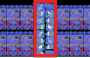
 With this motivation, Alan explored some of the on-chip options offered by Analog Bits. He provided an example to illustrate the scope and flexibility that can be achieved. The example, shown on the right, provides autonomous clocking of multiple SerDes protocols integrated on TSMC 16FFC technology with a combined clock unit. This example illustrates multiple rows of Analog Bits SerDes and seven coils of independent LC PLLs, each capable of driving a different frequency with a different spectral modulation to any of tens to hundreds of SerDes.
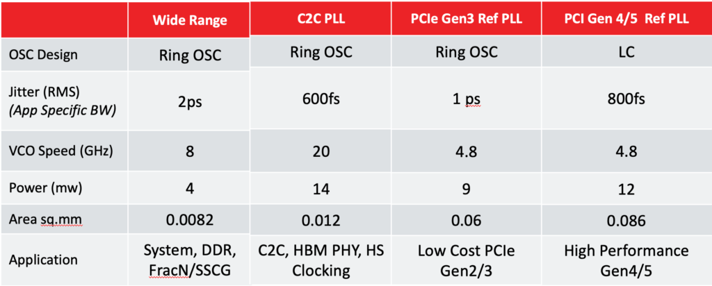
Central to a high frequency clock generator is a high performance PLL. Alan provided several examples of the types of PLLs supported by Analog Bits. These technologies provide a range of jitter, speed, power and area for various applications. Some, such as the LC oscillator design, work best only at high frequencies. The figure below summarizes the various options.

Alan then illustrated several examples of Analog Bits clocking solutions for various applications in several technologies. These included:
- A ring-based chip-to-chip clock generator in TSMC N7
- A PLL for cost-sensitive applications supporting PCI Gen 2/3 data rates
- A PCIe Gen 5 reference clock in TSMC N7/6
Silicon measurements of spread spectrum PLLs in TSMC 16FFC were presented. The data showed very good correlation to simulation results. Data for best-case conditions (FF wafers, high BW, high VCO amp) and worst-case conditions (SS wafers, low BW, low VCO amp) was presented. Closed-loop transient noise vs. silicon data was also reviewed.
Regarding collaboration with TSMC, Alan described an N6 test chip that taped out in June 2020. On board was a large complement of Analog Bits IP, including:
- Ring OSC PLL
- LC PLL
- Bandgap
- OSC pads
- RC oscillator
- TX/RX IO’s
Alan described the customizable architectures available from Analog Bits to clock numerous protocols, including:
- 16FFC: PCIe 3/4, SATA, SAS3/4, XFI, 10—KR
- N7/N6: PCIe 3/4/5 and can be expanded to other protocols
- N5: Available soon for PCIe 4/5, SATA, Ethernet
Clearly, Analog Bits provides a complete on-die clock subsystem for PCIe Gen 5 and beyond. Alan concluded by stating that Analog Bits has been a long-term partner of TSMC, providing a wide range of popular mixed signal IP for many applications. You can learn more at https://www.analogbits.com.
Also Read:
AI processing requirements reveal weaknesses in current methods
7nm SERDES Design and Qualification Challenges!
Share this post via:


Comments
There are no comments yet.
You must register or log in to view/post comments.