Application Processor SoC integrates more and more functions, generation after generation, challenging performance, cost, power efficiency, reliability, and time-to-market. But the maximum die size can’t increase, at least because of the constraints linked with wafer production, manufacturability, yield and finally SoC cost. The growing number of wires required to make connections to the different IP blocks within the design are generating new challenges at EDA level: Place and route (P&R) tools efficiency should ideally strictly follow Moore’s law, increasing by 40% when passing from 40 nm to 28 nm, to support identical SoC size. Starting such a discussion between EDA experts would certainly take long time before converging…
Let’s deal today with a surprising and positive finding: packet-based network-on-chip (NoC) interconnect fabric alleviates routing congestion. It has been proven that the top semiconductor design teams, who are building the most highly integrated chips, are addressing congestion by adopting NoCs for the interconnect. The increase in net count and total wire length to route plagues design teams with routing congestion. The drawbacks are so significant that they often negate the performance, cost, power efficiency, reliability, and time-to-market advantages of chosen IPs. This can cost chip companies opportunities for critical design wins in high-volume or emerging-growth markets.
As already mentioned, the place and route (P&R) stage of chip design is critical for reducing wire congestion. I have personally supported design team in charge of Supercomputer chip designs spending weeks if not months, stacked at Floor-planning stage (the design phase just before P&R, where you have to successfully position the most critical chip blocks, to increase your level of confidence that the next stage could be successfully passed).
During Floor-planning, you don’t effectively route the chip, but you get a very accurate view of a very important parameter: routing congestion. If the block positioning is not optimized, you will generate routing congestion. The result is not necessary a chip impossible to route, but certainly a chip larger than expected, that is, more expensive and consuming more power (P = CV[SUP]2[/SUP]), the wire capacitance being directly linked with the wire length. You could expect that adding metal layers will solve the problem, in fact it doesn’t: the chip size may not increase, but the cost will, as well as the wire capacitance, then power.
To summarize, designers must design for constraints on:
- Die size
- Power consumption
- Latency
- Metal mask layers
- Defect rate
- Wire lengths
- Mask costs
- Critical paths
- MTBF reliability
- Schedule
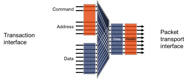
The interconnect fabric is the IP with the most significant effect on all of the constraints. The top semiconductor design teams, who are building the most highly integrated chips, are addressing congestion by adopting Network on Chip (NoCs) for interconnect the various chip functions, the many IP. This is because packetizing allows information to be sent sequentially with configurable degrees of serialization. This allows the throughput requirements of links within the chip to be met with a minimum amount of wire metal.

Figure 1: Packetization places the address and control signals on the same wires as the data.
Packetization and serialization reduce the size, and also maximize the temporal utilization of the buses connecting IPs.
- Packetization takes the SoC transaction data and places them on the same wires as address, control and command signals. This results in fewer wires to move data around on the chip compared with using standard socket or transaction interfaces.
- With serialization, the data can be transmitted on even narrower channels, thus shrinking wire count on chips. Designers can also trade wires for throughput and transaction latency to gain a greater degree of freedom compared to standard interconnect designs.

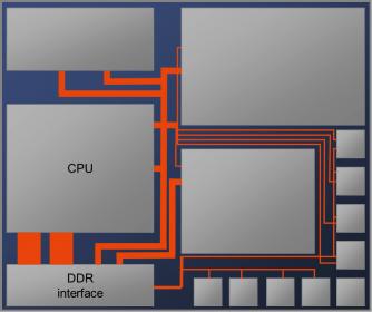
Figure 2: Packetization and serialization reduce the total wirelength of the top level interconnect by 50%.
Arteris thinks that serialization and packetization can cut in half the total wire length of the top-level interconnect fabric to route within a chip. If you want to know more, just have a look at this article.
From Eric Esteve
lang: en_US
Share this post via:


Comments
0 Replies to “How to reduce routing congestion in large Application Processor SoC?”
You must register or log in to view/post comments.