About 35 years ago the first commercial SPICE circuit simulators emerged and they were quickly put to work helping circuit designers predict the timing and power of 6um NMOS designs. Then we had to limit our circuit simulations to just hundreds of transistors and interconnect elements to fit into the RAM and complete simulation runs over night. Today we can enjoy using our smart phones with 5.7″ displays that are using FinFET nodes at 16nm and 14nm, but what kind of SPICE circuit simulator do circuit designers need to be using? Let’s start out by looking at an idealized FinFET and note the 3D nature of the transistor, especially how tall it has become:
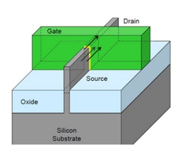
FinFET 3D structure, Source: Intel Corporation
Some of the new challenges with FinFET design are:
- The number of device parasitics have increased
- Layout rules are more complex and prohibitive
- Device noise must be included for accurate analysis
- Model evaluation is more compute intensive
- SPICE simulation run times are increased
Many consumer and industrial applications are already using the 16nm and 14nm FinFET technology for chips used as application processors, graphics processors, FPGAs and Memory. The typical trade offs occur in both FinFET and planar CMOS technologies: power versus speed versus area versus reliability. To reach your market window on time it is important to have EDA tools and a methodology that are up to the challenge.
Consider designing a PLL (Phase Locked Loop) circuit, the device noise must now be included for closed loop PLL phase noise analysis or else your results are too inaccurate (~30dB difference):
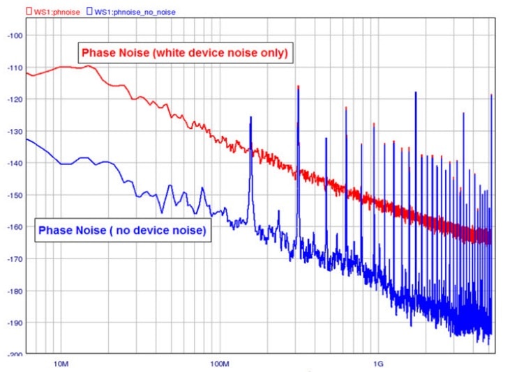
PLL Analysis must include device noise
Device noise is now a first order effect for FinFET transistors, so it’s an added type of modeling required for noise sensitive designs. Adding device noise will slow down the simulation speed of a SPICE circuit simulator.
Going back to the initial example of a smart phone which is battery-powered, we know that circuit designers are minimizing power to extend the battery life by using power gating, adding read/write assist circuits, and using multiple operating voltages. All of this circuit complexity impacts on-chip variations that lead to a jump in the number of PVT (Process, Voltage, Temperature) corner simulations required:
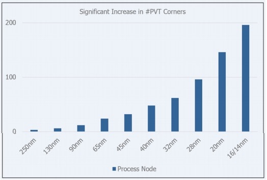
Number of PVT corners increases at 16nm, 14nm
With FinFET transistors the physical layout has more parasitic RC elements than planar transistors that need to be extracted and simulated in SPICE, plus there are more coupling capacitors, which tend to bog down SPICE circuit simulators even more. LDE (Layout Dependent Effects) contribute to longer running circuit simulations, and the following chart depicts the parasitic complexity increases as a function of smaller geometries:
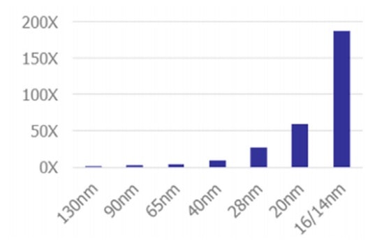
Parasitic complexity versus process geometry
On the reliability front we know that FinFET transistors can degrade over time by a few effects:
- Hot Carrier Injection (HCI)
- Positive Bias Temperature Instability (PBTI)
- Negative Bias Temperature Instability (NBTI)
With thinner dielectrics being used in FinFET designs the effects of device aging will actually increase the voltage thresholds for P and N channel devices, plus the channel carrier mobility will slow down, both which make the circuit perform more slowly and even shortens the circuit lifetime. These aging effects need to be simulated in SPICE to understand the reliability impact.
Analog FastSPICE
The good news is that the SPICE circuit simulator from 35 years ago has been dramatically re-architected to address each of these issues raised so far when designing with FinFET transistors. Just two years ago Mentor Graphics acquired the company Berkeley Design Automation and their Analog FastSPICE circuit simulator to better serve the needs of designing with FinFETs. Planar transistors have been simulated with standardized models like BSIM4 from UC Berkeley, however for FinFET transistors a new model called BSIM-CMG had to be used to account for the 3D nature and new effects:
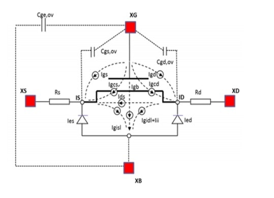
BSIM-CMG model, Source: University of California-Berkeley
This new BSIM-CMG model can run 2X slower than the previous BSIM4 models, but thanks to the new optimizations in the Analog FastSPICE (AFS) tool you can expect accurate results while using the same memory during simulation.
With AFS as your circuit simulator enjoy the modern architecture that gives you more than 120 dB dynamic range, speedier results than other SPICE simulators, uses multithreading for best sequential runs, handles 10M plus elements, and allows verification of full circuits including parasitics.
Read the complete White Paper online, or jump straight to AFS product details.
Related Blogs
- For high-volume manufacturing at 10 nm and below: technology and friendship
- Test Driving Analog/Mixed Signal Design for the Internet of Things
- Device Noise Analysis, What Not to Do for AMS IC Designs


Comments
0 Replies to “How 16nm and 14nm FinFETs Require New SPICE Simulators”
You must register or log in to view/post comments.