The second day (more like a half-day) of EDPS was devoted to 3D ICs. There was a lot of information, too much to summarize in a few hundred words. The keynote was by Riko Radojcic of Qualcomm, who has been a sort of one-man-band attempting to drive the EDA and manufacturing industries towards 3D. Of course it helps if you don’t just have a sharp arrow but the wood of Qualcomm behind it. Curiously, though, Qualcomm themselves have been cautious in actually using 3D IC technology. Possibly they have done some test chips but I don’t know of any parts that they have in production. Other presentations were by Altera, Mentor and Cadence, plus a panel discussion.
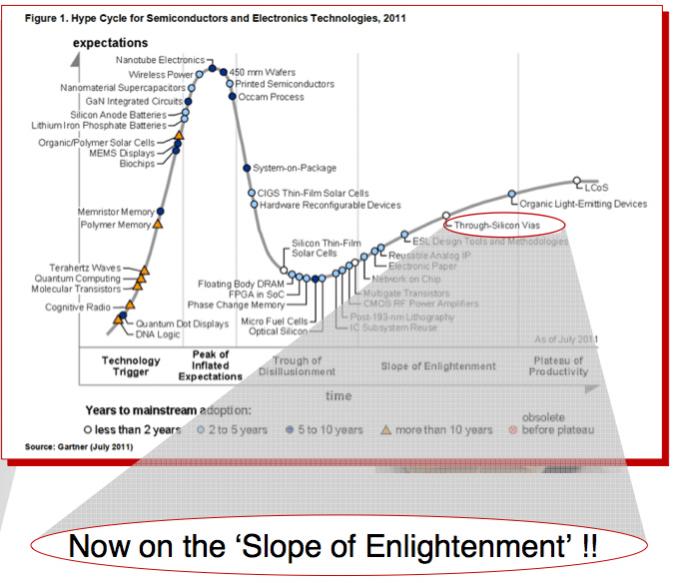
 Those who have been in hi-tech for years know about the hype cycle, I believe originated by Dataquest. Gartner, Dataquest’s heir, reckons TSV are now on the slope of enlightenment where things become real. At the top of the hype cycle are nanotube electronics, wireless power and Occam processes (whatever they are).
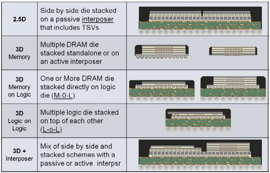
There are a number of varieties of 3D IC with different challenges for both EDA and manufacturing. If you include package-on-package (POP) then you probably have a 3D IC in your pocket. Almost all the smartphone SoCs including Apple’s A4/A5 series, have memory and logic in the same package. POP does not require Thru-Silicon-Vias (TSVs) since it is all wire-bonded inside the package.
One thing I learned is that while everyone talks about copper TSVs, the small TSVs that are so far in use are actually tungsten. Nobody knows how to make copper TSVs that small. There is actually a reasonable possibility that we will end up with two types of TSV: tungsten for signal, small and tightly spaced, and copper for power supply and perhaps clock, much bigger and with higher current capacity.
 One big development earlier this year was the finalization of the Jedec Wide I/O standard which allows memory to be stacked on top of logic, so called memory-on-logic (MOL). With much shorter distances, lower capacitance and 512 bits wide this allows a much higher bandwidth lower power interface between the processor and memory. The memory is also designed to be stacked, with more than one memory die. In fact all the memory suppliers have already announced various forms of memory stacks.
Interposer based designs, so called 2.5D, have the big advantage of not requiring TSV except through the interposer itself (unless there is a memory stack). As everyone who watches 3D ICs probably knows, Xilinx is shipping a high-end FPGA using silicon interposer technology, perhaps the only high(ish) volume product in production.
All camera chips are also 3D of some sort, with the CCD device on top of the image processing chip. There was an inconclusive debate as to how many of these use TSVs and how many use another technology whereby the signals are brought around the edge of the thinned die rather than going through it.
Thermal is going to be a big issue. Mobile chips are low power but they are not that big, so the power density and thus many of the thermal problems are the same as for server CPUs. IBM is looking at liquid cooling through microchannels. That has its own set of challenges and may or may not work out, but for sure that is not going to be the solution in your phone.
The motivation for 3D is a mixture of economic and what has come to be called “More than Moore”. We can no longer continue to scale CMOS the way we have been doing, and we are falling off the 30% per year cost reduction treadmill. It is still an open question whether we have a post optical lithographic process that we can manufacture economically, EUV being the most promising with E-beam the only other serious alternative. High-density TSV and 3D stacking offers an alternative way to keep Moore’s law on track (think of Moore’s law as being about transistors per volume, just that we only used one die for the first 50 years). It is the first of several disruptive technology changes that substitute for just scaling our lithography.
 But, as with any disruptive technology, you don’t get it for free. It is disruptive. You need new tools, a new supplier ecosystem. There are new sorts of interactions you need to worry about such as where TSVs can be placed, how they affect silicon through stress, managing electrical and thermal coupling in the stack and…and…
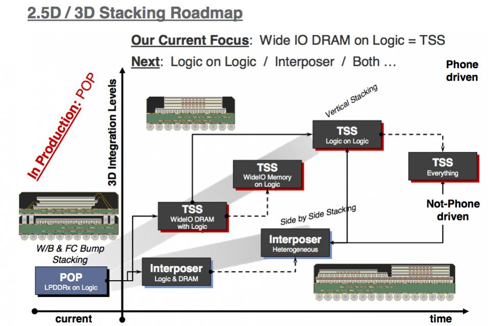
The roadmap, at the highest level, goes through POP (in production today), to wide-I/O MOL and eventually LOL.
Share this post via:


Silicon Insurance: Why eFPGA is Cheaper Than a Respin — and Why It Matters in the Intel 18A Era