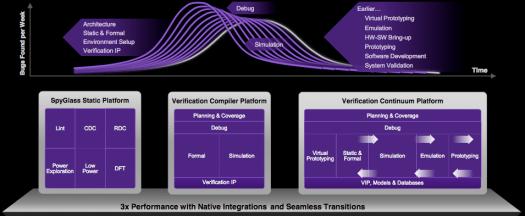
Unless you have been living in a cave for the last several years, by now you know that “Shift Left” is a big priority in product design and delivery, and particularly in verification. Within the semiconductor industry I believe Intel coined this term as early as 2002, though it seems now to be popular throughout all forms of technology development.

The idea behind Shift Left in verification starts from a difficult mismatch between traditional product flows and current market needs. A long-favored approach to design and verification has been to make these stages more or less serial, only starting serious verification on a phase of design when that phase is nearing completion. In more relaxed times, that approach was eminently sensible – why spend much time in test if what you are testing is still evolving?
But as designs become more complex, they also become harder to test, leading to more unpredictable verification closure. Semiconductor companies are now responsible for a lot more software content in the product, so verification spans both hardware and software. Also, product design is becoming a lot more collaborative – general-purpose catalog parts may still be around but the real money-makers are frequently co-developed; as a result, spec/requirements may continue to evolve through design.
All of which means that verification has to be pulled in earlier in the design cycle – the Great Shift Left. Sadly, appeals to fairness (the spec changed, you didn’t allow enough time in the schedule, you didn’t give us enough staff) don’t wash. Competitors are stepping up to shift left and delivering outstanding products on these crazy schedules. Buckle up; it’s natural selection time.
How can you push verification left when the design/assembly is still in flux? By moving more verification responsibility into design, or verification teams closely aligned with design. An increasingly popular way to do that is through is better smoke-testing (so the verification team doesn’t waste time on basic bugs) and coverage help (why can’t I get past 90% coverage on this block?).
Also of note, an important advance mentioned in the webinar is that SpyGlass looks like it is fully integrated into the Synopsys verification flow. You can start from a design compiled for VCS and you can setup to automatically switch into Verdi for debug. It’s getting a lot easier to stay in these fully integrated environments, which can’t be good news for the smaller verification players. VCS, VC Formal and other verification solutions leverage the same unified compile and debug environment.
Webinar Summary
With increasing complexity in chip designs, IP and SoC teams are faced with the challenge of minimizing risk, while still maintaining high levels of productivity. Poorly coded RTL is a primary concern, as it leads to bugs, longer verification cycles, unpredictable design processes and delayed time to market.
The combination of static and formal technologies enables smarter, faster and deeper lint analysis at RTL for early signoff. These advanced capabilities enable designers to perform a series of even more comprehensive checks, ensuring fewer bugs, a more stable design flow and accelerated verification closure.
In this webinar, Synopsys discusses how SpyGlass® Lint Turbo, VC Formal™ Auto Extracted Properties (AEP) and Formal Coverage Analyzer (FCA) Apps identify RTL issues at their source, pinpoint coding and consistency problems in the RTL descriptions, and help designers resolve issues quickly before design implementation. The webinar also shows a tool demo on the easy-to-use Verdi® unified debug capabilities, low noise technology to automatically find RTL bugs, dead code, unreachable FSM states and transitions using advanced static and formal technology.
You can watch the webinar HERE.
Share this post via:


Comments
There are no comments yet.
You must register or log in to view/post comments.