Choosing a memory architecture can be a daunting task. There are many options to choose from, each with their own power, performance, area and cost profile. The right choice can make a new design competitive and popular in the market. The wrong choice can doom the whole project to failure.
Vadhiraj Sankaranarayanan, senior technical marketing manager, Solutions Group at Synopsys has published a technical bulletin that should provide a lot of help and guidance for your next memory decision, especially of it’s focused on low power (which almost everything is these days). Entitled Key Features Designers Should Know About LPDDR5, Vadhiraj’s piece explores the advantages of a popular new JEDEC standard, LPDDR5.
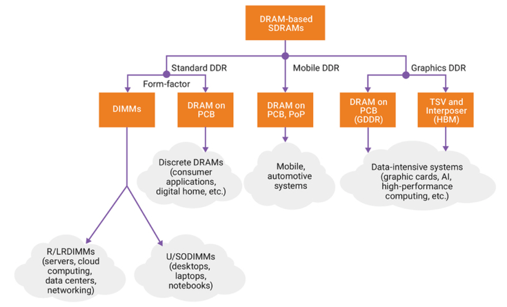
Before getting into some of the details of LPDDR5, Vadhiraj provides a good overview of the choices available today and some of the history regarding how these options evolved. You can get all the details by reading the piece, but suffice it to say there are a lot of choices, each with a long list of pros and cons.

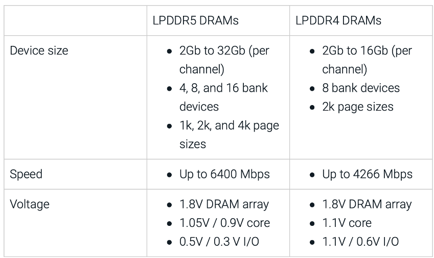
The balance of the piece discusses the details of LPDDR5, highlighting its features and diving into how many of those features work. The LPDDR specification addresses the middle piece of the diagram, above – Mobile DDR. As stated by Vadhiraj, “LPDDR DRAMs provide a high-performance solution with significantly low power consumption, which is a key requirement for mobile applications such as tablets, smartphones, and automotive.” The best way to understand the benefits of a new standard is to compare it to the previous generation. Doing that with LPDDR5 vs. LPDDR4 yields the diagram, below. More flexibility, more capacity, more speed, less power.

You can learn a lot about the architecture and benefits of LPDDR5 by reading Vadhiraj’s technical bulletin. To whet your appetite, here are some interesting facts about LPDDR5:
- Dynamic voltage scaling (DVS) is a method to modify, on-the-fly, the operating voltage of a device to match the varying needs of the system. LPDDR5 supports two core and I/O voltages through DVS (1.05V and 0.5V) for high-frequency operation and 0.9V and 0.3V for lower frequencies
- LPDDR5 adopts a new clocking scheme, where the clock runs at one fourth the data-strobe frequency at speeds higher than 3200 Mbps, and at half the data-strobe frequency at speeds under 3200 Mbps
- Decision feedback equalizers (DFEs) reduce inter-symbol interference on received data to improve the margin. LPDDR5 DRAMs have a single-tap DFE to improve the margins for the write data, thereby enhancing the robustness of the memory channel
- Write X is a power-saving feature that allows the transfer a specific bit pattern (such as an all-zero pattern) to contiguous memory locations very quickly. LPPDDR5 supports Write X
As mentioned, you can learn a lot more from Vadhiraj’s technical bulletin. Synopsys provides additional resources on the topic. There is a white paper on DDR SDRAM memories and Vadhiraj conducted a webinar on DDR5 and LPDDR5 that can be viewed as well.
Also Read:
Hybrid Verification for Deep Sequential Convergence
Edge Computing – The Critical Middle Ground
Share this post via:


Comments
There are no comments yet.
You must register or log in to view/post comments.