As more AI applications turn to edge computing to reduce latencies, the need for more computational performance at the edge continues to increase. However, commodity compute engines don’t have enough compute power or are too power-hungry to meet the needs of edge systems. Thus, when designing AI accelerators for the edge, Joe Sawicki, the Executive VP for the IC EDA Division of Siemens, at last month’s AI Hardware Summit in Santa Clara, Calif., suggests that there are several approaches to consider: Custom hardware that is optimized for performance, high-level synthesis to radically reduce design cost, and hybrid verification to significantly reduce validation cost.
When these approaches are combined, designers can craft high-performance AI accelerators for edge computing applications. That high performance will be needed since model sizes of the AI algorithms are growing over time—over the past five years, explained Sawicki, the models (such as the ImageNet algorithm) have increased in computational load by more than 100X and that growth shows no sign of slowing down.
Industry estimates from International Business Strategies show that the AI value contribution to the overall IC market revenue will grow from today’s 18% to 66% by the year 2030, while the total IC market revenue will grow from $529 billion today to $1144 billion by 2030. The gain in AI value demonstrates the increasing momentum in custom accelerators to improve both edge device performance and overall AI performance. Although the customized accelerators can deliver exceptional performance, they have one drawback – they have limited flexibility since they are typically optimized for a limited number of algorithms.
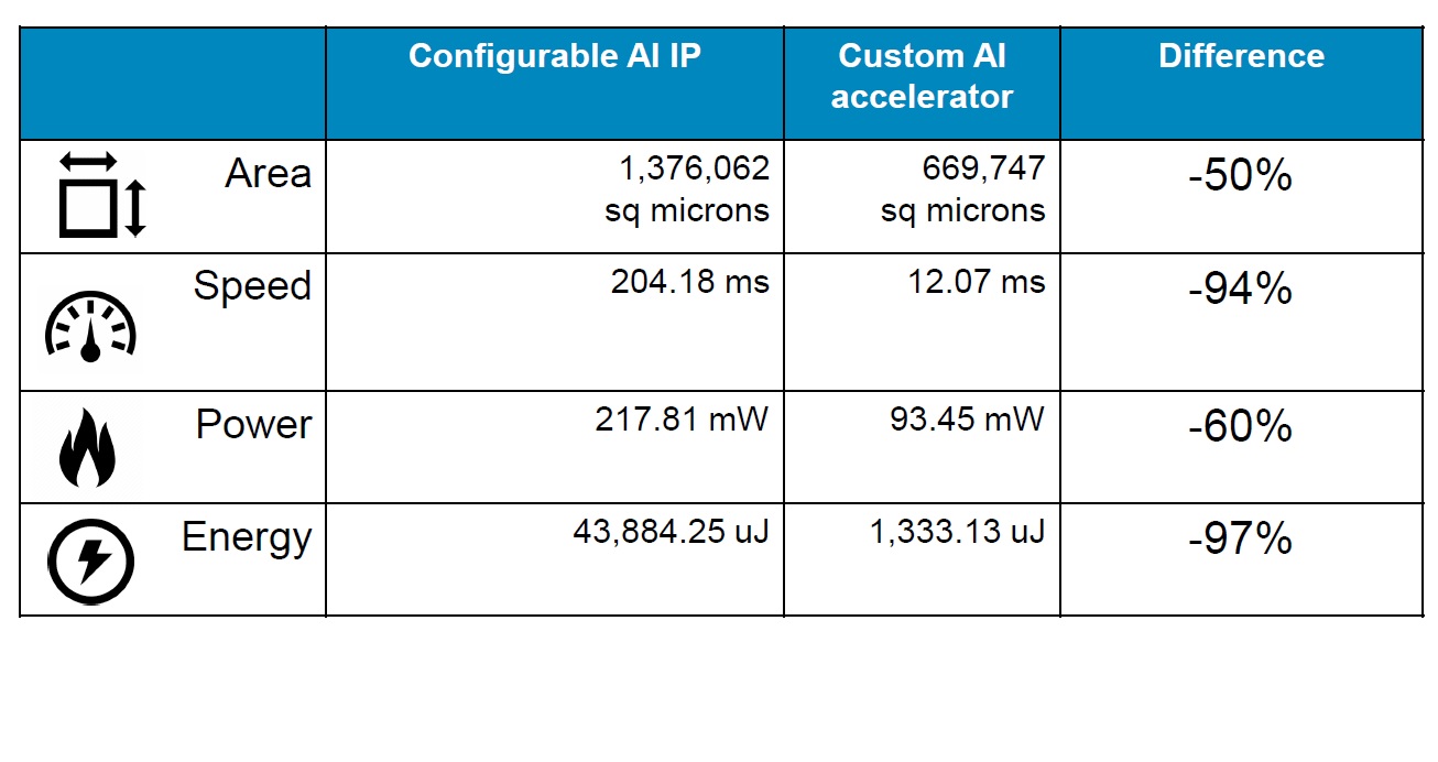
In an example described by Sawicki, a configurable block of AI intellectual property is compared to a custom AI accelerator design. Area, Speed, Power, and Energy all show significant reductions for the custom accelerator (see table). For example, area is 50% smaller, speed improved by 94%, power dropped by 60%, and energy consumed per inference was reduced by 97%. It’s not magic here–it’s because the architecture was specifically targeted to implement the specific algorithm explained Sawicki.

Part of the optimization challenge is to determine the best level of quantization—for example, 32-bit floating-point accuracy is often preferred, but with just a small loss in the result precision, a 10-bit fixed-point alternative that saves 20X in area/power can be used instead, thus improving compute throughput and reducing chip area. Additionally, by applying high-level synthesis in the hardware design flow, designers can go from the neural network architecture to a C++ bit-accurate algorithm to a C++ Catapult architecture and on to high-level synthesis to craft a synthesizable RTL design that can be implemented using RTL synthesis tools and back-end tool flows.
The use of C++ allows designers to easily explore various architectural approaches, suggests Sawicki. In a second example, he described the design exploration of a RISC-V Rocket core and three design options in a 16-nm process—one that is optimized for low power using an accelerator plus the Rocket core, a second that focused on shrinking the core area to minimize silicon cost, and a third approach that was optimized for speed. For the low-power option, the core plus accelerator consumed 86.54 mW, ran at 25.67 ms, and occupied a total area of about 3 million square microns. The second option reduced the total silicon area by about one-third to 2 million square microns, slowed down the execution to 37.54 ms, and kept the power to just under 90 mW. Lastly, the speed optimized version upped the area back to about the same level as the first option, improved the speed to just 12.07 ms, but upped the power consumption to 93.45 mW. These tradeoffs show that design choices can considerably affect the performance and area of a potential design.
The incorporation of AI/ML function in an EdgeAI design also adds additional verification challenges. The verification tools must deal with the training data set, the AI network mapping, as well as the AI accelerator logic (the structured RTL). As Sawicki explained, functional benchmarking has to deal with virtual platform performance, modeling of the hybrid platform, and simulation/emulation of the modeling platform. And all through that the tools must also perform power and performance analysis. To do that, the verification technology has to be matched to the needs of the project—hybrid verification and run-fast/run-accurate (ability to switch between model fidelity in a single run) make it possible to test real-world workloads in the verification environment.
By using open standards Sawicki expects designers to leverage a rich ecosystem of modeling capabilities in a heterogeneous environment for multi-domain and multi-vendor modeling. Tools for scenario generation, algorithmic modeling, TLM modeling and physics simulations can all be tied together via a system modeling interconnect approach that allows analog and digital simulation, hardware assisted verification through the use of digital twins, and virtual platform models to interact.
https://eda.sw.siemens.com/en-US/
Also Read:
Why Use PADS Professional Premium for Electronic Design
DFT Moves up to 2.5D and 3D IC
Siemens EDA Discuss Permanent and Transient Faults
3D IC – Managing the System-level Netlist
Share this post via:


Comments
There are no comments yet.
You must register or log in to view/post comments.