
PCIe design complexity continues rising as the standard for intrasystem communication evolves. An urgent need for more system bandwidth drives PCIe interconnects to multi-lane, multi-link, multi-level signaling. Classical PCIe design workflows leave designers with most of the responsibility for getting the requisite interconnect details right. These classical workflows also defer compliance testing until physical realization – when it can be too late to fix unforeseen chip problems. Keysight is revamping the PCIe design workflow with smart workflow automation in System Designer for PCIe®, including IBIS-AMI model generation and simulation-driven virtual compliance, speeding design cycles and reducing risk in a shift-left approach. We discussed the technology with Hee-Soo Lee, Director of High-Speed Digital Segment at Keysight.
Replacing tedious setups and hard debugging with workflow automation
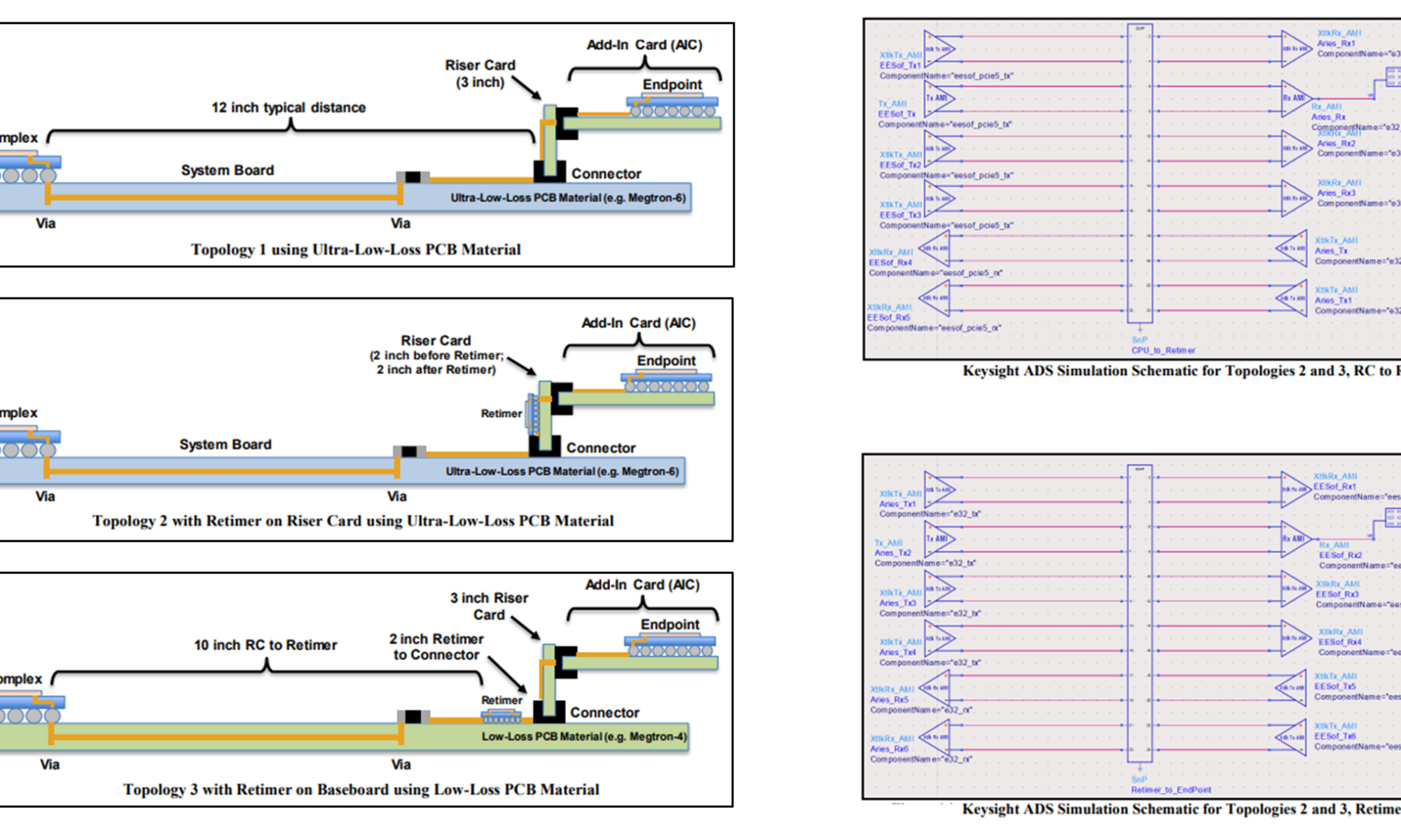
Traditional high-speed digital design requires PCIe designers to complete tedious manual design setups. In the example below, designers face a choice of whether to use a retimer (RT) and where to place it in the signal chain between the root complex (RC) and the endpoint (EP). Many scenarios benefit from using an RT, introducing two schematics, one between the RC and RT and another between the RT and EP, requiring individually wired signal connections from S-parameter blocks to signal drivers. Creating all the connections for complex multi-lane, multi-link designs can be very tedious.

Parameter sweeps in conventional high-speed digital simulations span many points, resulting in large data sets, and gathering insights becomes time-consuming. If eye diagrams from the analysis are closed, debugging channel performance is the first step, but it becomes a problem as the connections around the S-parameter blocks must be unwired and manually terminated for further simulation. Measurement probes also require manual insertion. Any mishaps in wiring or unwiring signals and terminations inject errors into debugging, requiring more investigation. If manual tasks like these become automated, designers can spend more time optimizing designs.
Lee contrasts this classical approach with the smart PCIe design workflow using Keysight’s Advanced Design System (ADS) and System Designer for PCIe®. “One schematic implements a topology with the RootComplex and EndPoint placed as smart components,” he says. “Smart bus wire makes all the connections accurately, automated with a click.” Below is the System Designer for PCIe® representation of Topology 3 above. Automatic placement of PCIe probes simplifies multi-dimensional data capture using smart measurement technology. What once consisted of hours of work in layout is now a few minutes, and preparing for and running a PCIe simulation is a few seconds.

Control over parameters and choice of simulations in one interface
Each of these blocks is configurable in the System Designer for PCIe® user interface. Expanding the example above to look at the PCIe Mid-Channel Repeater block shows some options. Designers can choose whether the block is a redriver or retimer, select how many differential pairs are in the link, and select an IBIS file for the model. Smart wire makes the connections with the correct parameters automatically. Designers can also set up bit-level system behaviors.

Simulation options from one schematic with no manual conversions also give control over the PCIe design workflow. Most PCIe designers are already familiar with Seasim, the statistical simulator from the PCI-SIG, which guides PCIe compliance evaluation. Existing workflows required designers to jump from their preferred simulation tool to the Seasim environment. When choosing Seasim simulation mode in System Designer for PCIe®, ADS characterizes the channels using its S-parameter simulator and launches Seasim (user-installed separately) from ADS for analysis.

In addition to the S-parameter simulator and the Seasim interface, two other simulation methods are available for selection in System Designer for PCIe®:
- A bit-by-bit simulator exercises sequences of bits specified in transmitters for durations specified in analysis settings, which helps analyze systems faster with waveform information embedded.
- A statistical simulator uses ADS proprietary algorithms to analyze random and periodic jitter, duty-cycle distortion, and other effects to achieve an extremely low bit error rate (BER).
IBIS-AMI modeling and virtual compliance evaluation
IBIS-AMI behavioral modeling for SerDes transceivers captures analog characteristics and algorithmic functionality such as equalization, gain, and clock data recovery. Millions of bits through a link can be simulated using convolution and data flow approaches in a few minutes.
Usually, a designer must have intimate knowledge of digital signal processing details and C coding to create an AMI model. With the PCIe AMI Modeler in System Designer for PCIe®, AMI model generation has become a simple task in the wizard-driven AMI modeling workflow. This capability is essential for cutting-edge PCIe Gen6 designs with multi-level PAM4 signaling, where AMI models may not exist yet. Output files include .dll for Windows or .so for Linux.

Finally, System Designer for PCIe® adds simulation-driven compliance. “Typically, PCIe compliance tests are done in the physical realm, using a detailed Method of Implementation in an oscilloscope application, testing performance against compliance metrics,” says Lee. “The problem is this is very late in the design cycle to discover for the first time if compliance tests pass or fail, and the risks are huge in complex designs.”
A guiding principle for Keysight EDA is using unified measurement science proven from hardware verifications in simulation-driven tests. The software that powers Keysight test equipment also runs in the Keysight EDA design environment – same algorithms, same methodologies. System Designer for PCIe® carries that principle to PCIe compliance testing with a specialized PCI Compliance Probe that sets up the correct stimulus and makes the appropriate compliance measurements. Users can accurately and thoroughly gauge PCIe design compliance from early-stage designs before committing to hardware.
This smart PCIe design workflow slashes the design cycle while providing faster insight into performance and a much earlier look at compliance. Keysight EDA is offering a deeper dive into System Designer for PCIe® and its capabilities in a webinar – registration is now open.
WEBINAR: Simplify Design Verification and Compliance with Standards-Driven EDA Workflows
More details are also available online: W3651B System Designer for PCIe®
Share this post via:


Comments
There are no comments yet.
You must register or log in to view/post comments.