
We’ve been covering the Dassault Systèmes “Silicon Thinking” platform for a while here, but, as I’m often prone to do, I wanted to explore the backstory to uncover more about the concept. With over 25M users of their product lifecycle management (PLM) solutions, why is Dassault Systèmes becoming so interested in semiconductor EDA?
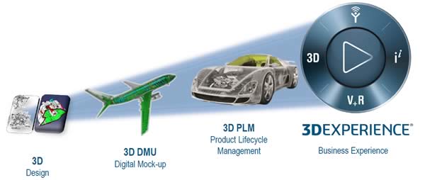
Most of that 25M user figure didn’t come from semiconductor design. Old timers may remember the beginnings – a product called CATIA, with origins around 1977. CATIA was a breakthrough in 3D computer-aided design, first finding widespread use in the aerospace and automotive sectors. From there, Dassault Systèmes evolved through four stages: 3D design, 3D digital mock-up, 3D PLM, and finally the 3D “business experience” of today.

The logic behind creating a “business experience” is simple. Products are no longer enough. We have moved from a commodities-based agricultural economy, to a products-based industrial economy, to a services-based economy, and are now in what many have said is an information-based economy. However, consumers don’t really buy information – they buy experiences. Consumers have a tighter link with producers, and are much more vocal in the cycle now.
Dassault Systèmes has unveiled a rather massive product line around creating and managing those experiences, the interaction between producers and consumers. I’m glad Dean Popowski, senior solution architect with Dassault Systèmes, explained the compass for me. I’ve seen this symbol dozens of times and never appreciated its meaning:
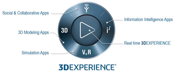
North points to social and collaborative apps, the category ENOVIA and the Silicon Thinking platform fall in to. West is the traditional 3D modeling apps. South is simulation, virtual plus real. East is information intelligence. The 3DEXPERIENCE is delivered through a web browser, with users purchasing capability through “roles” which expose more features. (For example, CATIA still has a thick client for full-strength design work, but other roles may see the same data via a much lighter browser interface.) The platform can be hosted on premise, in a public cloud, or in a private cloud.
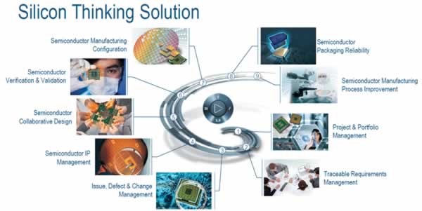
What does this all have to do with semiconductor EDA? Increasingly, the process of large chip design is becoming less about schematics and RTL, and more about a whole set of surrounding issues in collaboration. These issues include requirements traceability, defect management, IP management, verification and validation, manufacturing configuration, packaging, and metrics and process improvement.
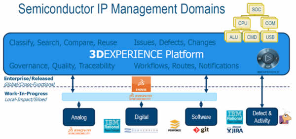
Dassault Systèmes often refers to “below the line” and “above the line” activity. Below the line is what we’d consider traditional design work with traditional analog and digital EDA tools, software tools, and defect tracking tools. Through the magic of a federation layer, databases underlying these tools can be brought together and exposed above the line for enterprise-level tasks.
For instance, suppose someone is asked to audit royalties on IP. You don’t really want to train that person on the digital EDA tool and expend a license on a seat they only use a fraction of capability of. In the 3DEXPERIENCE platform, they come in through a hierarchy tuned to their role delivering just the information necessary from the enterprise repository.
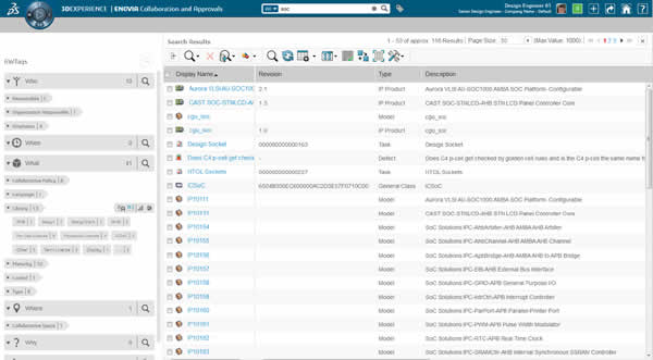
Popowski launched into a demo, and just one screen shot doesn’t do it justice here. However, a few important points emerge quickly. First, users log in by selecting a role, which configures the layout and context of the 3DEXPERIENCE tool. One option is for the login location to be tracked, which can trigger IP export controls (like ITAR classifications).
The left side of the platform is navigation, presented in 6WTags – who, what, where, when, why, and how – that support filtering of information. For instance, on this view of IP blocks, one can choose the library tag “ICSoC” and get a filtered view with just those blocks. Drill downs expose properties, hierarchy, actions, lifecycle, news, solutions, and subscriptions that trigger notifications when some event happens in a block. There are project schedules with Gantt charts and phase gate views, and status dashboards which show tasks at a glance.
3DEXPERIENCE brings together development work with enterprise IP management. Users collaborate based on roles instead of just apps, and are presented context to accomplish tasks efficiently. An end-to-end view facilitates IP reuse and helps govern projects from requirements to manufacturing.
Ultimately, the power of the 3DEXPERIENCE solution is in the ability to quickly customize designs faster by not reinventing the wheel each time. This is why Dassault Systèmes has been moving into semiconductor space. While the design and fabrication technology is different, complex semiconductors are no different from airliners, cars, or other complex systems composed of IP blocks assembled in some process. With systems functionality now strongly tied to electronics and software, it’s a logical step in the evolution of Dassault Systèmes.
Also Read
Latest Pinpoint release tackles DRC and trend lines
Sustainability, Semiconductor Companies and Software Companies
The Mechanical Reliability of IC Packages
Share this post via:


Consolidation and Competition: Who is Winning the $4.5 Billion Interface IP Race?