Once upon a time, one wireless base station (BTS) was expected to support one, and only one wireless protocol, like GSM (2G), first deployed in Finland in 1991, or CDMAOne (also 2G) developed by Qualcomm and released through the TIA in 1995. Just a precision: the GSM modem speed was reaching 14.4 Kbps (with only 9.6 Kbps usable by end-user) as well as the CDMAone competing technology…
Such a modem was already supported by a DSP core (Teak from CEVA or TI’ C54x), but you have now to figure out what kind of DSP is needed today to support the following requirements:
–Facilitate aggregation of various technologies such as LTE, LTE-A PRO, WiFi 11ac/ax, WiGig…
–Reduce Latency (to best support V2X, VR or mobile gaming)
–Support huge numbers of users and IoT devices at once (you can translate it into supporting massive MIMO technology)
–Enables mission critical usage such as Cellular V2X, eHealth and industrial IoT (reliability and encryption)
supporting modem functions is still part of this DSP charter, but the speed of modems are now ranging from 20 MHz to 800 MHz, depending on the protocol!
In fact, the above description if for such a wireless standard (5G) is so advanced compared to previous generation that it needs a completely new processing approach to ensure its success…
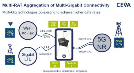
In this picture, the key-word is aggregation, as the CEVA XC-12 targets the base station segment rather than the smartphone irself, where the CEVA XC-4500 is powerfull enough to support 5G modem gigabit requirements. In the BTS, multiple multi-gig technologies are co-existing and some of the protocols to be supported by the DSP are still to be finalized. In this case, the DSP based approach is certainly this providing the highest flexibility to implement the modem baseband. As well, it’s likely that the digital RF will be implemented through FPGA technology.
On top of increased flexibility, another strong benefit going with using the CEVA XC-12 is the reuse capability. Building a BTS is costly, as OEM have to target high performance (IP and technology node) for the highest possible number of end-users. Selecting the XC-12 allows to this OEM to add new H/W while keeping in place the previously installed system.
Let’s take a look at the new computing challenges associated with 5G adoption:
·Computational complexity is very high: higher throughput, reduced latency and massive MIMO usage
·Need for minimum mean square error (MMSE) equalization of huge matrices requiring very efficient matrix operations
·High precision to handle large matrix inversion is essential for Equalization and Beamforming calculation
·Data symbol demodulation as high as 256-QAM if not 1024-QAM!
·The larger bandwidth, modulation and MIMO dimensions automatically leads to much higher bitrates
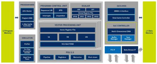
The CEVA XC-12 architecture has been specifically developed to address all the above listed challenges. Taking the CEVA XC-4500 as a reference, here are some improvments on the symbol plane. 128-MAC used to boost 8×8, 16×16 or 32×32 MMSE-IRC by 4X factor and 20-bit Pseudo-FP to boost Massive-MIMO by more than 20 dB. FFT automatic scaling improving precision by 15 dB enabling 4X performance…
At this stage, I suggest you to attend to the Webinar to be hold on March, 29[SUP]th[/SUP] 2017“How CEVA-XC12 solves the daunting computing and latency challenges of 5G NR” (you will find the link at the bottom of this blog).
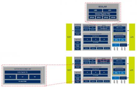
Each of the four vector engines can run 32 MAC per cycle, for a total of 128 MAC per cycle, and supports 2048-bit load and store, still per cycle. The high precision fixed and floating point arithmetic has been defined for up to 256×256 matrix processing (remember the MMSE equalization requirement). Vector engines are supporting high precision non-linear ISA and 256, or even 1024 QAM demodulation ISA.
The scalar unit, completely new and based on the new CEVA-X framework (CEVA-X1, CEVA-X2), is designed for Multi-RAT systems and management of massive number of users to best support 5G BTS. Each of the four Scalar Processing Unit (SPU) can optionally integrate a Floating Point Unit (FPU).
Compared with the CEVA-XC 4500 scalar unit, the new scalar unit offers 40% EEMBC improvement (the EEMBC CoreMark benchmark reflects real-world applications and tests a processor’s basic pipeline structure, as well as the ability to test basic read/write operations, integer operations, and control operations. It tend to replace the old Dhrystone MIPS benchmark).
As the CEVA-XC 12 counts 4 SPU (and 4 VPU), the CEVA-XC 12 provides a 4X improvment for a complete BTS NR PHY. This SPU provides full RTOS support, offering ultra fast context switch.
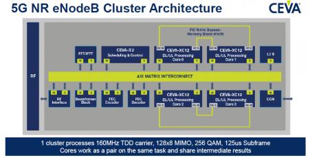
The above picture illustrate how the CEVA-XC 12 is implemented. This Cluster Architecture allows the CEVA-X2 to control the complete system. The four processor cores are connected by paires (Core 0 with Core1, Core 2 with Core 3) by using point to point Fast Interconnect busses (FIC Master or Slave). Each paire is processing in parallel the same task and because of the point to point (and fast) interconnect, the latency is greatly improved, which is a condition to efficiently address the Virtual reality (VR) or Vehicule to Everything (V2X) applications.
To conclude, let’s add that the CEVA-XC 12 has been implemented in 10 nm technology and can reach up to 1.8 GHz in this case. For Multi-RAT control plane, the core delivers 4.4 CoreMark/MHz, while consuming 50% less than the CEVA-XC4500.
You will certainly learn and benefit from the webinar to be hold on March, 29[SUP]th[/SUP] 2017:
“How CEVA-XC12 solves the daunting computing and latency challenges of 5G NR”
Register at:
http://go.ceva-dsp.com/Webinar-XC12-29-3-17_1-LP.html
Product Brief:
http://www.ceva-dsp.com/assets/docs/downloads/CEVA-XC12-Product-Brief.pdf
Landing page url:
http://launch.ceva-dsp.com/CEVA-XC12/
Product page url:
http://www.ceva-dsp.com/CEVA-XC12
By Eric Esteve from IPnest


Comments
There are no comments yet.
You must register or log in to view/post comments.