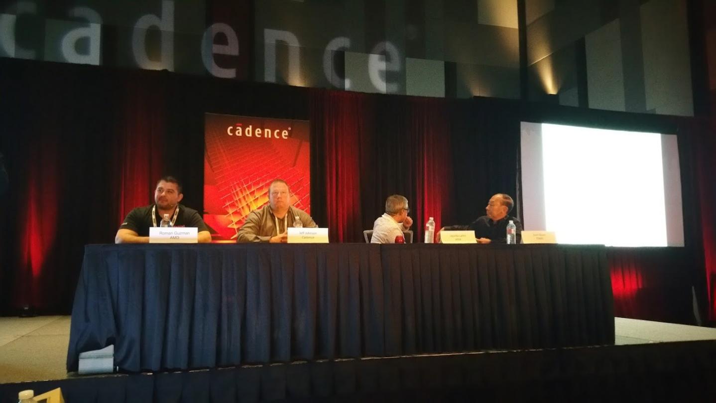
IC design challenges are different at advanced nodes like 7nm, so to learn more about the topic I attended a panel luncheon at DAC sponsored by Cadence. The moderator was both funny and technically astute, quite the rare combination, so kudos to Professor Rob Rutenbar, a former Neolinear guy now at the University of Illinois. Panelists included the following people:
- Roman Guzman, Mask Designer at AMD
- Jayanta Lahiri, Physical IP group at ARM
- Tom Quan, Marketing at TSMC
- Jeff Johnson, Engineering Director at Cadence

Panel Discussion
Q: What are your biggest IC layout challenges using advanced nodes?
A: (AMD) Physical verification, learning all of the rules, because it takes so much time to iterate and reach a clean layout.
A: (Cadence) The DRM used to be understandable, but now you don’t know what’s wrong or how to fix it, very complex with FinFET. Complex rules causes 4-5 DRC runs to reach closure.
A: (ARM) FinFET allowed us to bring down voltage levels to 1.1V, however the number of PVT corners went way up (100 PVT combinations), and on the plus side we can now do 8 input gates with FinFET.
A: (TSMC) We define advanced node as 28nm and smaller. With the move to 20nm it required double patterning, a new challenge from planar. In the move to 16nm we used the same BEOL as 20nm, however now when we use FinFET devices it requires 3D extraction, EM for high current, LDE, resistance increased, Fin quantized W values, Fin grid spacing. Moving down to the 10nm node we see full coloring required. With the 7nm node we will need triple or quad patterning on some layers and there are new density issues.
Q: What do you spend most of you time on?
A: (AMD) Physical verification and EM/IR fixes, this is very tedious work.
Q: Are automation tools working for your IC layouts?
A: (Cadence) Yes, with Pcells, SDL (Schematic Driven Layout) and now device generators for FInFET we have a new methodology that is saving layout time.
A: (ARM) The variation in the processes is quite high at 0.6V, requiring more simulation efforts, so improvements are needed. Today we have separate timing and power closure, which is too slow, so why not one step to achieve both timing and power closure?
A: (TSMC) There are lots of new layout rules for FinFET, so automating the layout process works for things like dummy fill, intelligent Pcells, block level automation. Challenges remain, like: Self heating slows down SPICE simulation times, LDE is not intuitive for layout design and analog layout, gradient densities, fixing EM/IR issues earlier. Early analysis is wanted to prevent closure issues, so we should be embedding prevention into tools.
Q: Where does your IP engineering team spend time?
A: (Cadence) With a higher ratio of physical designers to logic designers on advanced nodes we see more time being spent on: device level placement, device level routing. We really cannot wait until the end to get DRC clean.
Q: What is the learning curve like for an IC design group doing their first FinFET products?
A: (ARM) Modeling and simulation required much learning for us, something like 3-4 months to get a handle on what views our IP group should be creating so that SOC designers can use them. With FinFET we used massive CPU and disk space compared to planar designs.
A: (TSMC) Circuit designers can come up to speed quickly to learn about using the correct number of fins instead of an arbitrary W/L ratio. At 10nm the full coloring is also something totally new.
Q: Why are customers going to advanced nodes?
A: (TSMC) Moore’s Law continues to drive why customers want smaller nodes, PPA with 2x density 40% less power, 40% speed improvements. FinFET brought high current drive, lower leakage, lower voltages. AMS designer always want better matching with FinFET, plus increased Fmax and higher Ft values.
A: (ARM) Voltage scaling stopped at about 28nm, so the newer FinFET helped on lower voltage and standby power. Not all ICs need FinFET.
Q: How to make your life easier for IC design?
A: (AMD) Make the IC routing more productive on P&R, providing interactive routing.
A: (Cadence) Automation to take care of complex rules. Simplify the problems for our designers, with fewer combinations offered.
A: (ARM) The number of views is too high in a FinFET process, plus the CPU and disk usage are still too high. Power and Timing closure should be done together, not separately. Reliability simulations are not adequate yet.
A: (TSMC) Work early with IP and EDA vendors to make the flow efficient, define the methodology and software needed. Achieve accuracy of models to match silicon measurements. The recommended methodology is captured in the reference flow.
Q: (ARM) The bit cell voltages are still too high, what can you do for us?
A: (TSMC) Maybe we need an SRAM panel session to get into that topic.
Q: Is there anything new coming from PDKs?
A: (TSMC) – We’re using Pcells with enough sophistication to be DRC correct (Modgen). The PDK can also have utilities to ensure correctness.
Q: Are there any issues with digital design at advanced nodes?
A: (ARM) We design digital cells with high fan-in now for FinFET, although this requires more MonteCarlo simulations for us.
A: (Cadence) We constrain our designers to preset topologies in order to reduce the workload. We are using the foundry supplied Standard Cells.
Q: What is you favorite advice to our audience of IC designers today?
A: (TSMC) FInFET design requires more physical designers, while your choices for layout become less. Use device generators to get the fastest methodology.
A: (ARM) Economics dictates if FinFET will work for you, so just get ready for some CPU and disk space increases.
A: (Cadence) Work to develop a simple methodology, instead of a complex one.
A: (AMD) Be prepared for Tequila shots, the rules are way complex, stress levels are high.
Summary
Of all the DAC panels that I’ve attended in 2016, I have to admit that this one had the best moderator and most lively interchange among the members. It really felt like the questions and answers were not just canned, but very much heartfelt, especially the last answer about FinFET designs requiring more Tequila shots because of the increased challenges.


Comments
0 Replies to “IC Designers talk about 28nm to 7nm challenges at #53DAC”
You must register or log in to view/post comments.