There’s an old adage, attributed to renowned computer scientist Andrew Tannenbaum, one that perhaps only engineers find amusing: “The nice thing about standards is that you have so many to choose from.” Nevertheless, IEEE standards arise from customer requirements in the electronics industry. Many relate to the definition of complex communication protocols, such as the emerging 100Gigabit Ethernet interface (100GbE). A recent version of this protocol standard — IEEE 802.3bj-2014 — added a 4-lane X 25Gbps physical specification for backplanes, connectors, and twinax copper cables.
The emergence of advanced, high data rate channels introduced the problem of how Tx/Rx chip IP developers and system designers could concurrently and independently proceed with their product implementations. A new facet to standardization was needed, to define how analysis of these channels could be pursued — the Channel Operating Margin (COM) methodology was defined, and incorporated into 802.3bj.
Recently, I had the opportunity to discuss the COM method with Cristian Filip, HyperLynx architect, and Chuck Ferry, HyperLynx Product Marketing engineer at Mentor Graphics. Their insights were most illuminating and informative.
Channel Analysis History
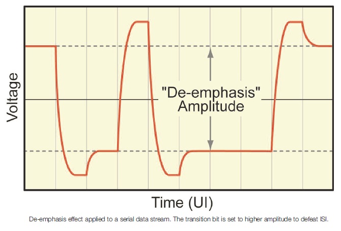
Early serial communications protocol implementations with effective lane data rates of 1-3Gbps — e.g., PCIe 1.0, SATA I — utilized a linear Feed Forward Equalizer (FFE) at the transmitter to provide de-emphasis to the sequence of bits in the data stream. The influence of adjacent data transitions to the desired transmitted value would result in inter-symbol interference (ISI) at the receiver end of the channel. To compensate for ISI, de-emphasis is added to the transmitted data signal voltage, as illustrated in the figure below.

(From Texas Instruments App Note 76W_19777)
Multiplicative tap values are applied to preceding post-cursor bit values D_i-1, D_i-2, … (and potentially, to pre-cursor future values D_i+1, …), and summed with the tap-multiplied D_i value to provide the differential-pair Tx voltages for the i_th unit interval. A shift register provides the various bit values that contribute to the signal. Summing current mirror circuits with tap-controlled series resistance legs are commonly used to provide the differential de-emphasis voltages.
Analysis of these early implementations involved examining the resulting signal at the Rx receiver pins, to measure how (frequency-dependent) channel losses, noise, and transmit jitter affected the waveforms.
An eye diagram comprising a single time unit interval overlay of a random bit sequence is an easy-to-interpret visual indication. The eye provides:
- a measure of the worst case ‘1’ and ‘0’ signals (and thus the required Rx reference voltage and sensing circuit offset limits)
- the time window for sensing, and
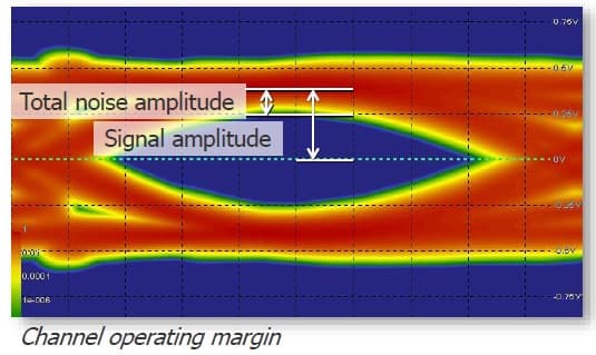
- the signal-to-noise measure (refer to the COM eye diagram figure below)
Tools evolved to assist designers extract frequency-dependent scattering parameter S-parameter models of the physical channel, and optimize FFE tap multipliers for a maximal eye opening by simulation of the time-domain behavior of the lane.
The next generation of protocols — e.g., PCIe 2.0/3.0, SATA II/III, USB 3.0, in the 3-10Gbps range — necessitated additional filtering and signal processing, to ensure low statistical bit error rate (BER) signaling. Specifically, the receiver end of the channel required additional equalization circuitry to open up the closed eye present at the Rx pins, ideally inverting the lossy frequency response of the physical channel. The Rx equalization architecture often uses adaptive techniques and a related bit stream training sequence to capture a suitable data signal inside the receiver.
A continuous time linear equalizer (CTLE) is a linear filter designed to attenuate low- and high-frequency signal content at the receiver, and amplify the content around the desired data rate frequency. (Note that the FFE at the Tx also effectively attenuates low-frequency content in the transmitted signal.)
A decision feedback equalizer (DFE) is also added to the receiver. It combines an FFE with additional summation of delayed, tap-multiplied past symbol values to further reduce ISI. At these data rates, on typical lossy channels, the smearing of the Rx signal due to ISI is severe — compensation for a greater number of data bit cursors is required.
Two key trends emerged for these protocols:
(1) An extension to the IBIS electrical model definition was defined — IBIS-AMI modeling support for FFE, CTLE, and DFE functionality now enabled full Tx-channel-Rx simulation. (Note that it is no longer sufficient to evaluate/simulate the eye diagram at the Rx pins, without equalization.)
(2) System designers needed a means by which they could proceed with implementation of the channel, separately from the Tx/Rx design (and IBIS-AMI model generation). A set of frequency-dependent loss budgets were defined:
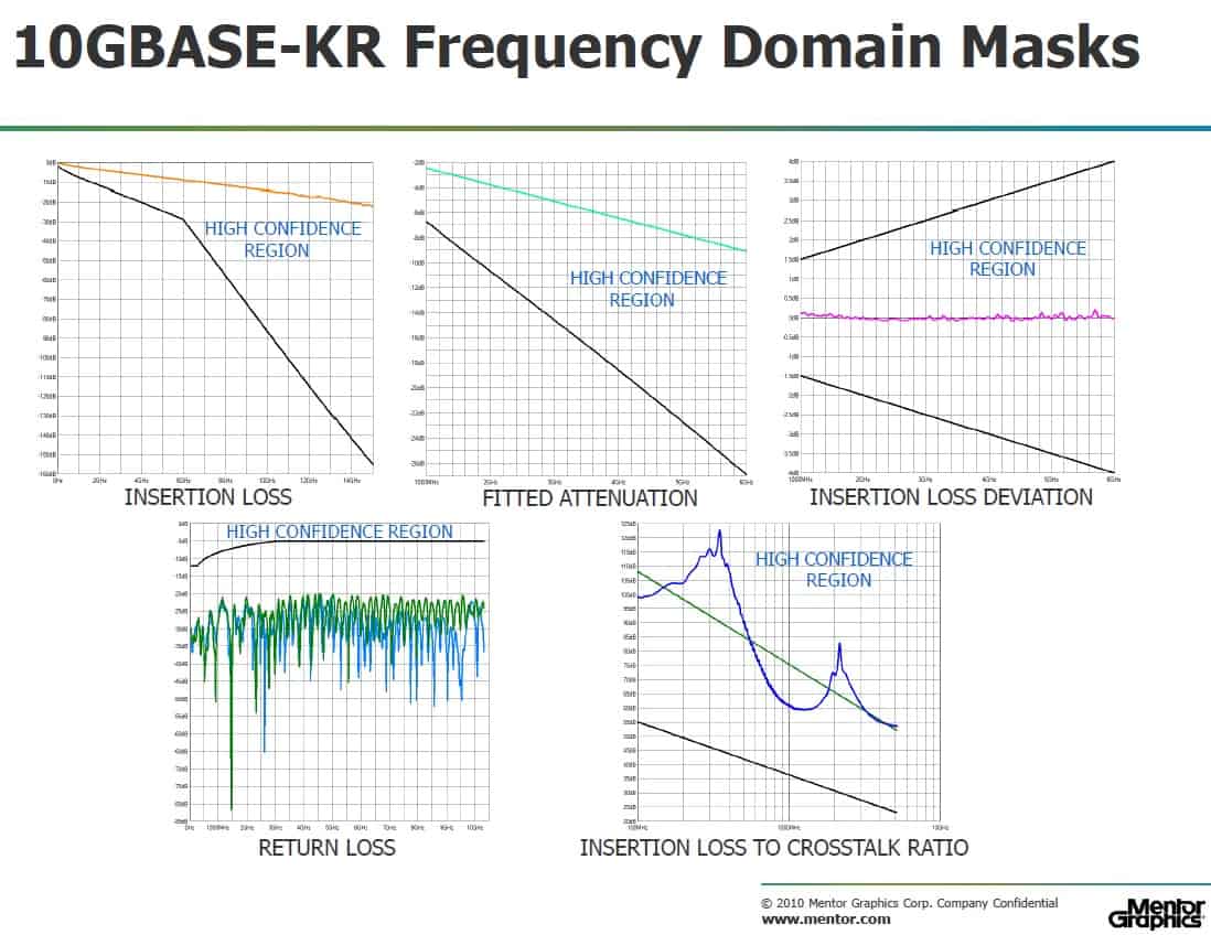
- insertion loss (IL)
- insertion loss deviation (ILD)
- reflection loss (RL)
- insertion-to-crosstalk ratio (ICR)
These maskscould be readily compared to the extracted S-parameter models of the channel, to see if the actual losses exceeded their specific budget — for example:
IL = -20 log |SDD21| in dB
(No single mask at the Rx pins is really viable at these data rates.) The figure below illustrates the masks for the 10GBASE Ethernet standard over a backplane.

However, failing a specific mask at a frequency related to the data rate (and its harmonics) does not necessarily imply an excessive BER; and, more significantly, passing all masks individually may not guarantee a suitable BER.
COM Methodology
Fast forward to today’s aggressive 25-28Gbps goals over traditional physical channels, as mentioned earlier for 100GbE. System designers still require a means to independently pursue channel implementation, ideally with a simpler approach than analysis of separate masks. The Channel Operating Margin methodology was developed, and adopted as part of the IEEE standard. (Mentor Graphics is a very active participant in this standardization effort.)
A reference architecture for Tx and Rx filtering and equalization is defined in the standard, which establishes the minimum functionality required from chip IP providers. Parameters for package models are included.
A single, overall COM measure for the channel is used, representing the signal-to-noise amplitude at the Rx pins, integrating the effects of loss, interference (near-end cross-talk, or NEXT, and far-end cross-talk, or FEXT), and statistical noise:
COM = 20 log (A_signal / A_noise) dB , at a BER = 10E-12
The figure below illustrates the COM measurement, using an eye diagram for illustration.

Note that the signal-to-noise ratio is more meaningful than just the eye opening alone — the additional context of the magnitude of the contributing noise on the channel signal is required, relative to the eye opening.
And, Tx/Rx and channel compliance to the COM definitions will have the added benefit of reducing over-design, from the perspective of both the IP and system designers.
Briefly, the COM methodology involves the following steps, starting with an S-parameter model:
- apply Tx/Rx filtering
- determine the resulting frequency-domain voltage transfer function
- execute an inverse FFT to determine the time-domain pulse response
- automatically determine optimal Tx FFE and Rx CTLE/DFE settings for the “victim” channel lane
- determine the equalization settings for the aggressor channels
- with the filter and tap settings set, convolve the time-domain responses to determine the overall waveform
Note that there is potentially some pessimism in the COM calculation, as all crosstalk aggressors are phase-aligned.
HyperLynx has automated and simplified the COM analysis flow:
- the user provides as input an S8p/S16p/S24p differential multi-port S-parameter model, with FEXT/victim/NEXT coverage
- the operating mode is set (e.g., 100GbE)
- a table of additional analysis parameters is defined (e.g., jitter)
- the COM analysis is executed
In addition to the Pass/Fail margin calculation, HyperLynx reports intermediate results from the calculations — e.g., channel step response, other time-domain waveforms, and the equalization reference settings.
A few additional comments from Cristian and Chuck were especially enlightening:
“COM applies to both Non-Return-to-Zero (NRZ) and multi-level (PAM) signaling protocols.”
“COM does not replace IBIS-AMI, which is still needed for the most demanding end-to-end simulations.”
“At these data rates, the importance of accurate multiport S-parameter models for boards, connectors, and cables is paramount. The COM standard specifies the required bandwidth and frequency step increments used to derive the S-parameter model. HyperLynx incorporates utilities to help assess S-parameter model quality. The connector/cable providers are focused on enabling this methodology with their models.”
And, relative to the future of the COM standard, they added:
“COM will clearly evolve to support future protocols — and, existing protocols are embracing COM, too. Within the methodology, package model support will be enhanced, including the option of user-specified package models. Jitter and crosstalk model support will be improved, as well.”
Clearly, the COM standard satisfies a crucial need in enabling and simplifying the implementation of high-speed SerDes protocols. HyperLynx provides system designers with an integrated analysis methodology.
Here is a link to a DesignCon 2016 paper from Mentor on COM, which provides an insightful comparison between the COM methodology and traditional statistical eye-based BER calculations.
-chipguy
Share this post via:


Comments
0 Replies to “Channel Operating Margin (COM) — A Standard for SI Analysis”
You must register or log in to view/post comments.