This year is shaping up to be an inflection point, when multi-die packaging technology will experience tremendous market growth. Advanced 2.5D/3D package offerings have been available for several years, utilizing a variety of technologies to serve as the package substrate, interposer material for embedding die micro-bump fan-out redistribution and interconnect metals, and (for 3D stacks) the method for fabricating vertical vias through intermediate package/die strata. Some recent examples include the Xilinx UltraScale product family (TSMC’s CoWoS technology) and AMD’s Radeon R9 integration of a GPU with stacked High Bandwidth Memory (HBM) die.
This year, the market growth will come from packaging technology enhancements directed at more cost-sensitive (read: mobile) applications. Wafer-level chip-scale packaging (fan-in WLCSP) has been extended to fan-out packages, and soon, fan-out multi-die solutions, as exemplified by TSMC’s recent InFO-PoP announcement.
Yet, the design environments for die and package implementation remain separate — i.e., distinct tools for chip vs. package physical design, distinct rulesets for DFM, distinct project databases and manufacturing data formats (e.g., GDS-II, Gerber). A unique technology is required to bridge these different domains, and provide an integrated design verification solution.
Recently, I had the opportunity to chat with John Park and John Ferguson at Mentor Graphics, about their approach to advanced packaging design enablement, and specifically, their participation with TSMC as a constituent of the “reference flow” for InFO-PoP. It was a most enlightening discussion.
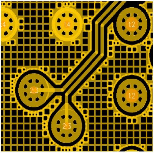
John P. emphasized the complexity of dealing with the chip and package implementation domains. He said, “For a designer coming from the chip world, the biggest technology difference for advanced packaging is the routing environment for fan-out and signal interconnects. These traces utilize all-angle geometries, circular vias, and unique teardrop and taper contours.”

He highlighted another complexity, stating, “For the aggressive fan-out technologies like InFO, there are intricate manufacturability rules for copper meshing and voids, to provide suitable mechanical stress relief to minimize warpage, and to alleviate copper pour outgassing issues.”
John P. went into additional detail, on how Mentor has extended their leading Calibre product capabilities to support advanced packaging technologies. “The key is the geometric data processing engines integrated into Calibre 3DSTACK, which were required by the WLP technology design kit from TSMC. Their design rules make extensive use of the equation-based DRC support in Calibre — which are similar to the complex rules in Photonics technology design kits. And, Calibre supports multiple designs in a single project, a requirement for these packages.”
He continued, “These features enabled TSMC to use GDS-II as the InFO data representation, and for the familiar Calibre sign-off for manufacturing release flow already used by customers. We also enhanced the GDS-II rendering support in our Xpedition product, to support using GDS-II.”
John F. added, “There’s a subtlety that we have to manage, as well — as there are separate sources for die and package data, there may be overloaded uses of manufacturing layer info. The flow ensures that there are no conflicts in layer references.”
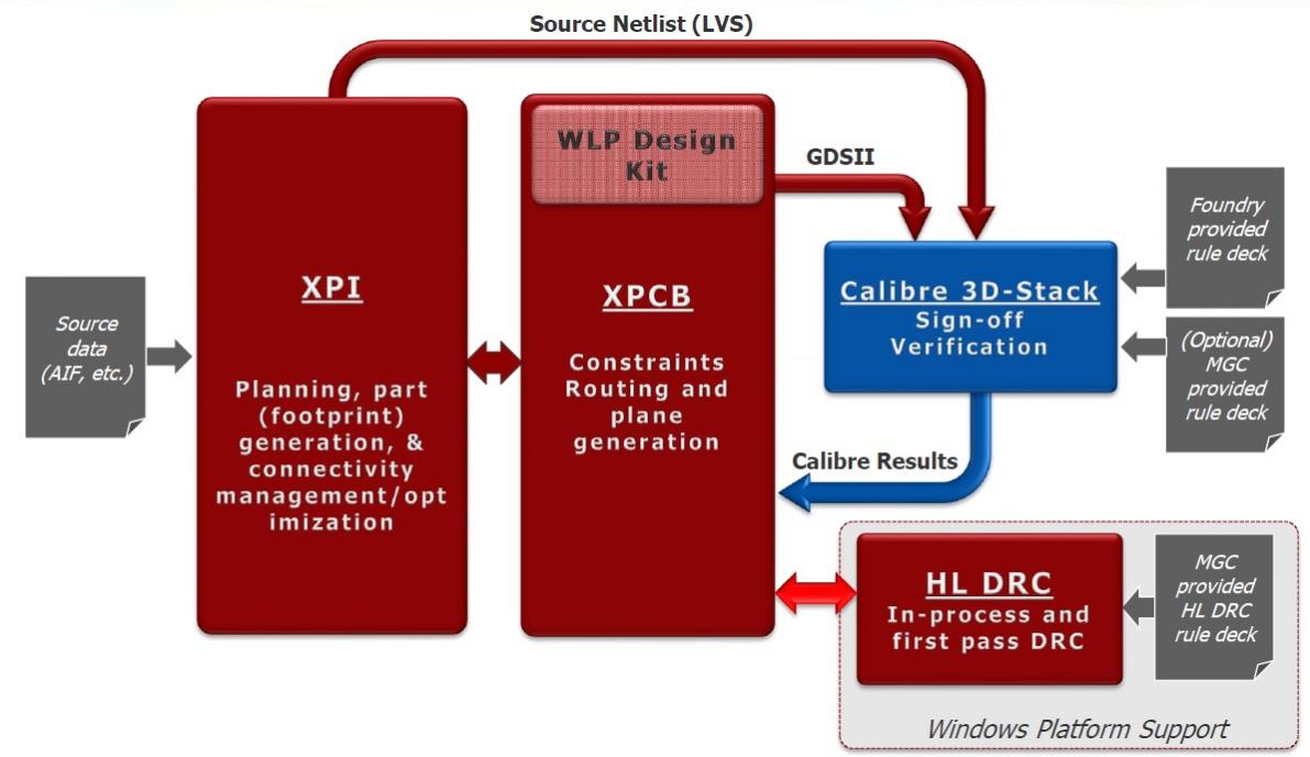
The flow for advanced multi-die package verification is appended below.

The initial step is to utilize the features of Xpedition Package Integrator (XPI in the diagram), which focuses on constructing the multi-die project connectivity model from the various, EDA-neutral, data formats. (An earlier semiwiki article described some of the features of XPI here.)
John F. added, “The Calibre 3DSTACK capabilities for multidie package verification are definitely not limited to Xpedition users; other environments are certainly supported (e.g., Cadence Allegro Package Designer, Zuken). For Xpedition users, there is the added benefit of an available WLP design kit utilizing Hyperlynx DRC, that enables designers to remain in the (Windows O/S) tool environment, to iterate more quickly.” (as depicted in the lower right-hand corner of the flow diagram)
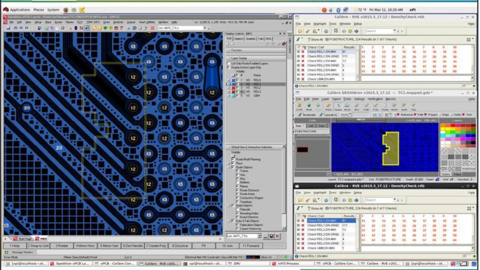
“Also, debug results from the (Linux-based) Calibre sign-off flow are directly integrated in Xpedition, with cross-probing between Calibre result and Xpedition geometry.” (illustrated in the figure below)

Our discussion concluded with the all-important reminder that these advanced packaging solutions require detailed thermal/mechanical stress analysis, another area where Mentor’s support excels.
The rapid pace of development for (low-cost, small form-factor) multi-die packaging solutions has necessitated a focus on providing reference flows for verification, that support interoperability in chip and package design environments. Mentor has addressed this requirement through extensions to their Xpedition product family, and through the introduction of Calibre 3DSTACK (which does not require a new license, by the way). Design kits and reference flows are available.
It will be exciting to see how end products released later this year will leverage this advanced packaging technology.
For more info on Calibre 3DSTACK, please follow this link.
-chipguy
Share this post via:


Comments
There are no comments yet.
You must register or log in to view/post comments.