IC layout parasitics dominate the performance of custom digital, analog and mixed-signal designs, so the challenge becomes how to identify the root causes and to quantify the effects of parasitics during early design stages. The old method of iterating between layout, extraction, SPICE simulation, followed by manual debug and analysis is just too slow and error prone to be relied upon. A smarter approach has been developed with an EDA tool called ParagonX from Synopsys, so I attended a recent webinar to become more informed. ParagonX came from start-up Diakopto which was acquired by Ansys, then Synopsys acquired Ansys.
Rob Dohanyos of Synopsys opened up the webinar with an overview of ParagonX and then most of the time was spent in a live demo, something kind of rare with EDA vendors. The ParagonX tool can be used by a circuit designer to analyze, debug, visualize and even optimize their IC layout parasitics for any technology node and any circuit design style. Typical users of the tool are designing high-speed or high-precision circuits, like: SERDES, optical transceivers, ADC, DAC, SRAM, clocks. Parasitic sensitive designs also benefit from this analysis: Analog, power nets, PMICs, ESD networks, guard rings. Smaller nodes benefit even more from ParagonX, all the way down to 3nm. Instead of spending weeks and months debugging parasitic effects, a designer can reduce that time to hours or minutes.
Circuit designers and layout engineers will find the new tool to be easy to use out of the box, with quick run times, while providing insights to any problem areas. Here’s where ParagonX fits into your existing design and layout flow:

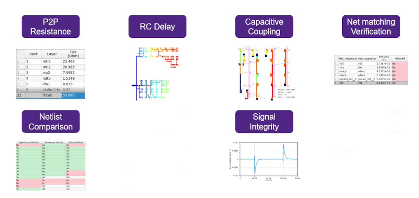
This tool can accept netlists that are hundreds of gigabytes in size and analyze nets that have hundreds of millions nodes or resistors, all made possible through it’s own binary netlist database. Users can expect fast netlist loading for top-hierarchy analysis, including power net analysis all while using the interactive GUI. There are six basic analysis features in ParagonX:

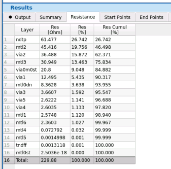
Invoking the tool brought up a GUI with choices grouped by analysis features, then they loaded a netlist in a few seconds. All nets could be traversed with a hierarchical widget, plus searching for nets with wildcards made it fast to find a specific net. Point to point (P2P) resistance was shown by selecting start and end points, and then the resistance contributions were displayed by layer type and percentage contribution.

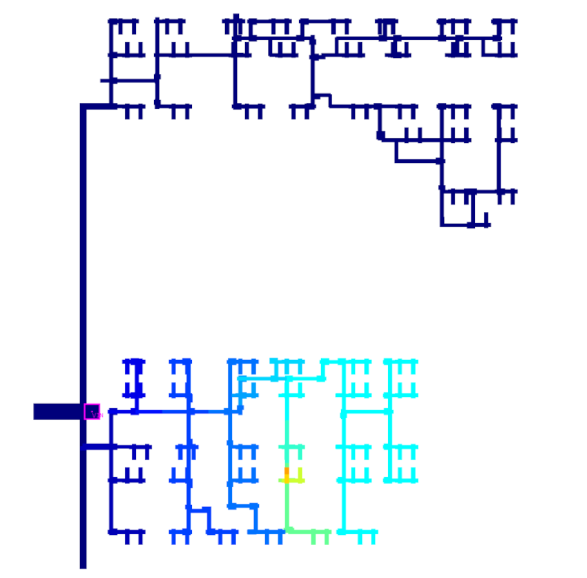
The top four layers had the most resistance, so next they showed sensitivity analysis with visualization of the layout by color-coded resistance.

Each of the many functions in the ParagonX tool are actually Pythons scripts that you can customize to fit your own analysis needs. From the command line of the tool you can see each script being used for a particular function. A function called Rview shows the resistance to all points on one net, and this got 1,000 times faster in the latest tool release. Rob ran Rview on a sample net VIN, showing 240 instance pins with a resistance distribution of 100 to 450 ohms.
Next in the demo the capacitive coupling on a single net was run on net VIN and all aggressor nets, showing that VSS had the most coupling from VIN to diffusion. Metal 3 had the highest coupling on VIN with CLOCK S. Users can tell which nets and layers are causing the most coupling, both numerically and visually.

RC delay was another function demonstrated with a start point of VIN to all instance points, then a device characterization file was generated for use with a specific SPICE tool. Sensitivity of RC delay to parasitics was the next function displayed using a rainbow of colors.
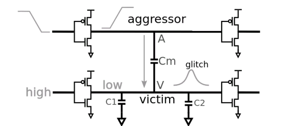
The net matching function was run on a differential pair, VIN and VIP, where the user set the matching criteria and simulation results showed layout areas in red that were not matching, while areas in green were matching properly. Several other functions were demonstrated: Layout Parasitic Screener, What-if analysis, victim noise analysis, glitch analysis.
Summary
Circuit and layout designers now have a much smarter way to quickly analyze IC layout parasitics, find the root cause and even begin to optimize their designs by using the ParagonX tool in their flow. This really is a new EDA tool category and will benefit custom-digital, analog and mixed-signal design projects.
Watch the archived webinar online.
Related Blogs
Share this post via:


Comments
There are no comments yet.
You must register or log in to view/post comments.