PCB and package designers need to be concerned with Signal Integrity (SI) issues to deliver electronic systems that work reliably in the field. EDA vendors like Siemens have helped engineers with SI analysis using a simulator called HyperLynx, dating all the way back to 1992. Siemens even wrote a 56-page e-book recently, Signal Integrity Basics, so I’ll capture the essence of that in this blog.
Signal Integrity
A digital designer can start out by assuming that a signal has a perfectly shaped waveform, but when they measure that signal as it propagates along a PCB or package to some receiver, the signal has analog distortions, like overshoot, plus there is a time delay to transit the interconnect.
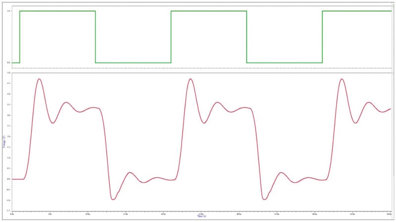
Overshoot comes from impedance mismatches and is followed by some ringing. Another waveform issue is Inter Symbol Interference (ISI), where bits sent over a channel start to interfere with each other, causing the receiver to ponder what the correct data is. Here’s what ISI looks like in a serial bit stream.
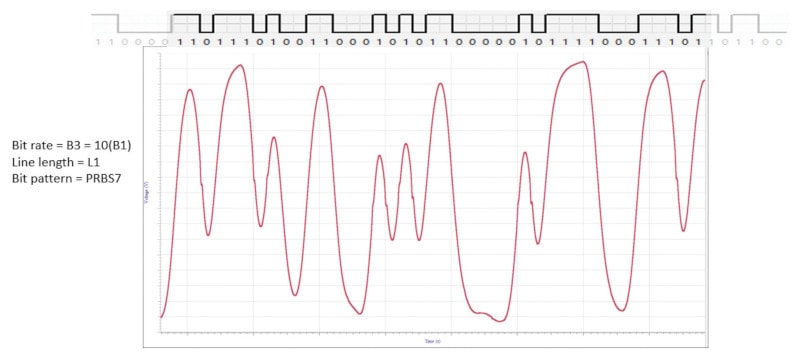
The bits are changing value so rapidly that the high and low level are not reaching proper values. The eye diagram for this channel has grown quite small, as the orange hexagon indicates, meaning that bit errors will be high.
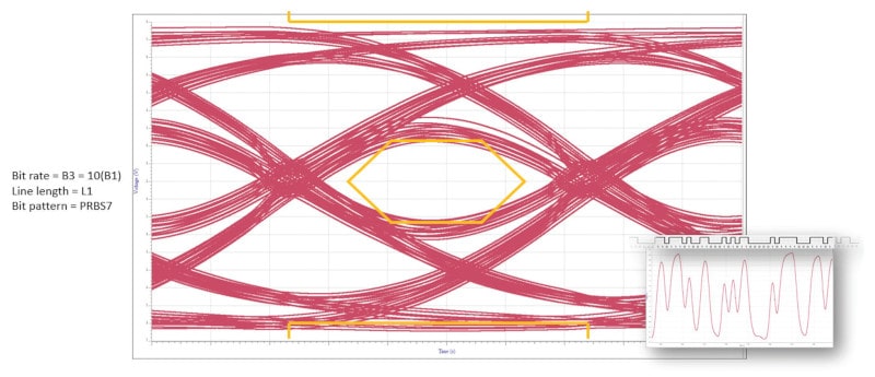
Increasing the length of the channel or increasing the frequency of the channel will close the opening of the eye diagram.
Interconnects used in PCB designs will always have delay, loss, and coupling, which then impact the signal integrity, so modeling this as a transmission line helps to understand and predict the behavior. The typical propagation velocity in a PCB is about 5.9 inches/ns. You can model a transmission line as a collection of resistors, inductors, and capacitors, in order to simulate and predict signal fidelity.
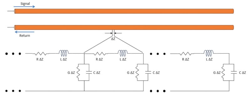
Two examples of transmission line types in PCB traces are microstrips and striplines. Delay and impedance along these transmission lines are impacted by the parameters of the particular trace. Delay along a microstrip is affected by the interconnect length, the dielectric constants, the height of the dielectric under the trace, and the width of the trace. Delay along a stripline line is affected by the interconnect length and dielectric constant(s). The characteristic impedance, Z0, for both of these transmission line types is impacted by the dielectric constant(s), the height of the dielectric(s) around the trace, and the width of the trace.
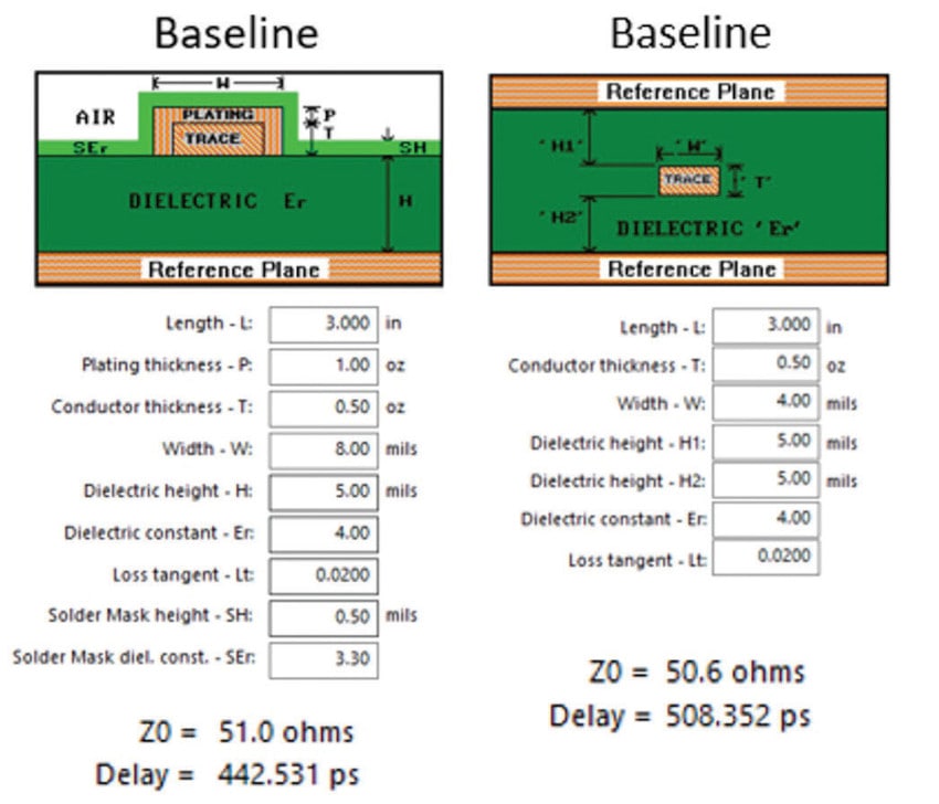
These examples used uniform cross sections, however changing the cross section of a trace can introduce an impedance discontinuity, which in turn causes reflections in a signal. The idea is to minimize and manage discontinuities, by:
- Using short interconnect, relative to rise/fall times
- Keeping consistent impedance along a trace
- Avoid or minimize vias
In the following example there’s a 3.3V CMOS driver and receiver connected by a 50 ohm transmission line with a 10ns delay from driver to receiver.
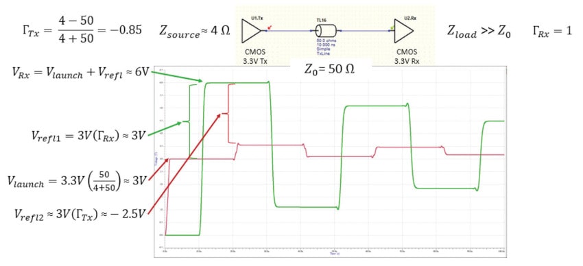
The driver is shown in Red, and it rises to 3V, short of the full 3.3V as there’s output impedance on the driver. As the signal propagates along the transmission line it reaches the receiver, which has a high impedance and reflection coefficient of 1, making the Green signal reach 6V. A reflected 3V signal propagates in 10ns back to the driver with a reflection coefficient of -0.85, which bumps the Red driver signal. These reflections continue to bounce back and forth, changing the Red and Green voltages as ringing.
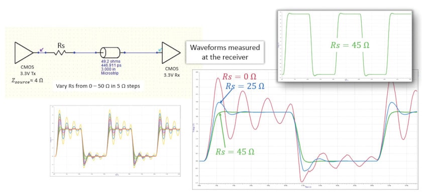
Adding a series terminating resistor close to the source driver can mitigate the overshoot and ringing as shown below:
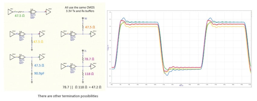
Parallel termination configurations can also reduce overshoot and ringing.
Multiple PCB traces placed in close proximity exhibit crosstalk, caused by capacitive and inductive coupling. Notice how the victim trace bounces around at the near end and the far end as the aggressor trace is toggled.
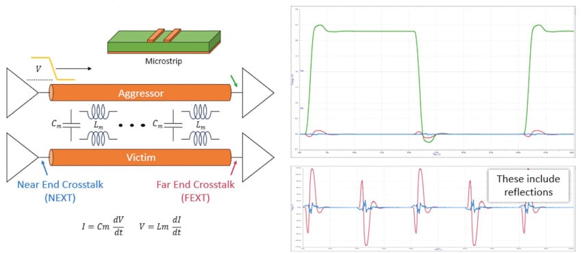
Adding termination to the traces will mitigate the bouncing, as does moving the traces farther apart, true for both microstrip and stripline configurations.
Differential Pairs
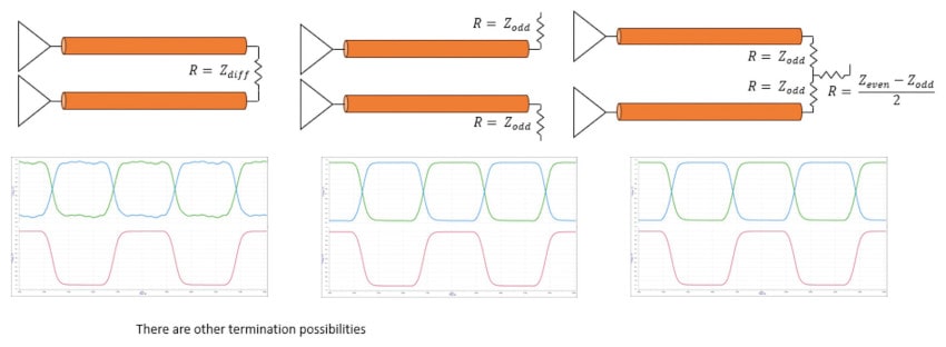
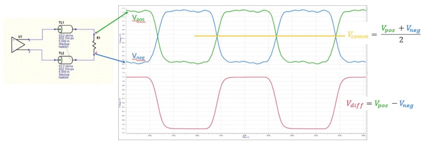
Another type of signal are differential pairs which have two complementary signals, Vpos and Vneg:
Even mode is when both signals are the same, while odd mode has opposite values on the signals. Three termination examples are shown which produce a cleaner Vdiff signal.
Vias
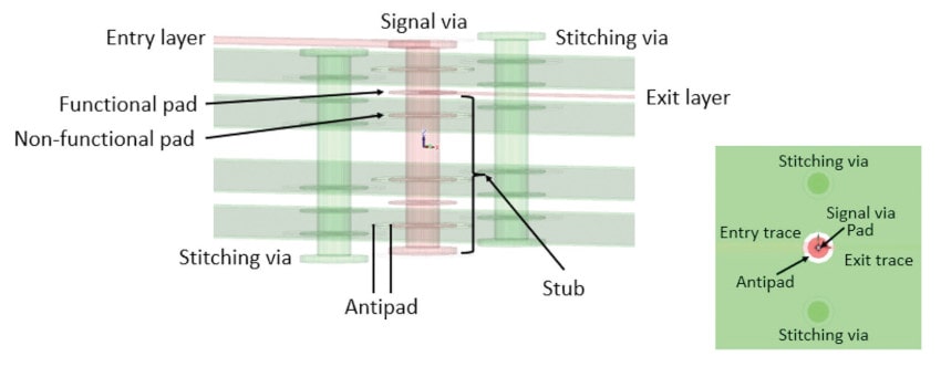
A basic via is shown below and the signal is in Red color, while the Green vias are stitching vias that connect reference nets together between layers.
Analysis of vias on a trace is done in the frequency domain using S-parameters and in the time domain using Time Domain Reflectometry (TDR). S21 is the ratio of the signal out of port 2 when injecting a signal into port 1, called insertion loss. S-parameters have both magnitude and phase components. S11 is the return loss.
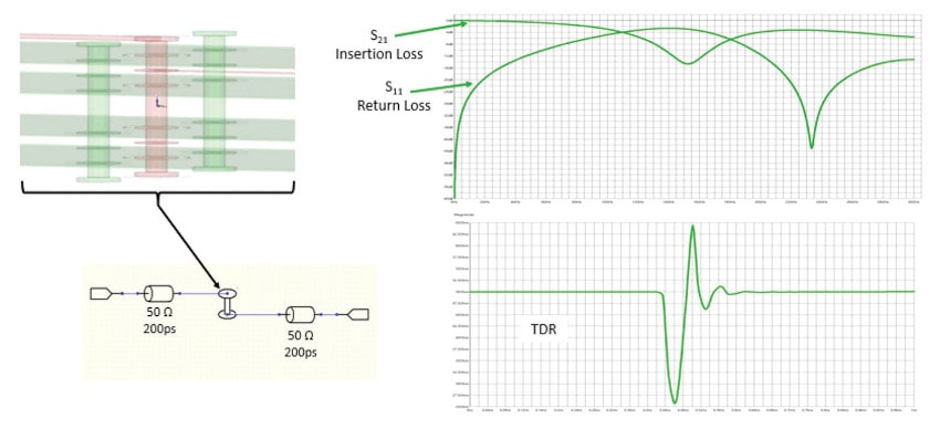
S21 – the insertion loss, has a dip at 15 GHz, from the stub acting as a quarter-wave resonator.
For the TDR plot it is flat on the left and right, corresponding to the two 50 ohm traces, and in the middle there’s a bounce in the impedance caused by the via.
A number of modifications can be made to a layout that affect via performance. The impacts of a few of these are investigated in the eBook: the presence of non-functional pads, the size of antipads, and stub length.
Timing
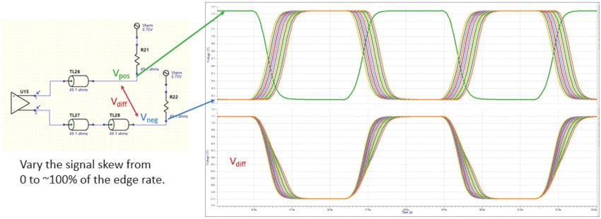
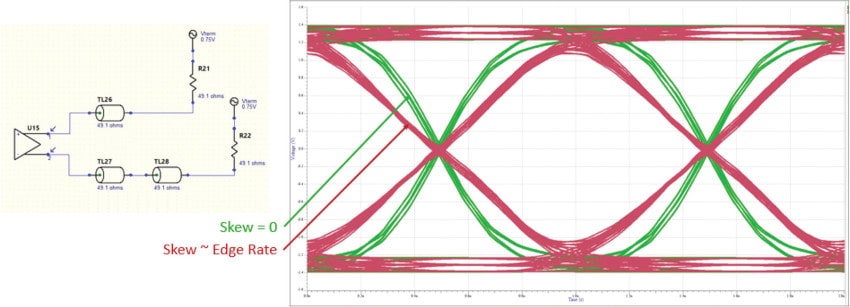
PCB traces are characterized by timing parameters like edge rates and propagation delay from a driver to multiple loads, which then impact setup and hold times for digital circuits. Consider the time difference in a differential pair, called skew, which changes the shape of Vdiff, caused by mismatches in the trace layouts. As the skew increases, then the edge rate of Vdiff slows down.
Increasing the skew also begins to close the eye diagram.
Summary
The 56 page e-book from Siemens EDA does a thorough job of introducing signal integrity concepts, challenges and mitigation approaches to PCB professionals. High-speed digital designs have challenges, and with understanding plus analysis, they can have reliable signals.
Read the entire e-book of Signal Integrity Basics, written by John Golding, Sr. AE Consultant, Siemens EDA.
Related Blogs
- Will my High-Speed Serial Link Work?
- Siemens Promotes Digital Threads for Electronic Systems Design
- Using PCB Automation for an AI and Machine Vision Product
- DDR5 Design Approach with Clocked Receivers




Comments
There are no comments yet.
You must register or log in to view/post comments.