At the DesignCon 2023 event this year there was a presentation by Micron all about DDR5 design challenges like the need for a Decision Feedback Equalizer (DFE) inside the DRAM. Siemens EDA and Micron teamed up to write a detailed 25 page white paper on the topic, and I was able to glean the top points for this much shorter blog. The DDR5 specification came out in 2020 with a data transfer bandwidth of 3200MT/s, requiring equalization (EQ) circuits to account for the channel impairments.
DFE is designed to overcome the effects of Inter-Symbol Interference (ISI), and the designers at Micron had to consider the clocking, Rx eye evaluation, Bit Error Rate (BER) and jitter analysis in their DRAM DFE. IBIS-AMI models were used to model the DDR5 behavior along with an EDA tool statistical simulation flow.
Part of the DDR5 specification is the four-tap DFE inside the DRAM’s Rx, and the DFE looks at past received bits to remove any ISI from the bits. The DFE first applies a voltage offset to remove ISI, then the slicer quantizes the current bit as high or low.
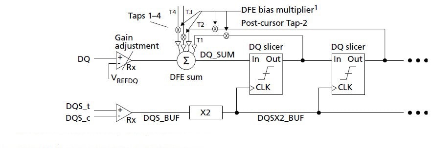
With DDR5 the clocking is a differential strobe signal (DQS_t, DQS_c), and it’s forwarded along the single-ended data signals (DQ) to the Rx. The DQS signal is buffered up and then fanned out to the clock input of up to eight DQ latches, causing a clock tree delay.
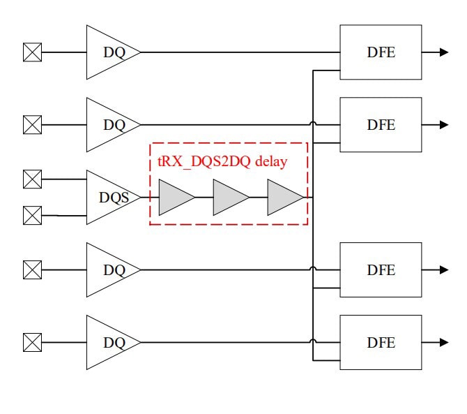
The maximum Eye Height is 95mV and the max Eye Width is 0.25 Unit Interval (UI), or just 78.125ps.. Using a statistical approach to measuring BER of 1e-16 is most practical.
IBIS models have been used for many generations of DDR systems, enabling end-to-end system simulation, yet starting with DDR5 adding EQ features and BER eye mask requirements, a new simulation model and analysis are sought. With IBIS-AMI modeling there is fast and accurate Si simulation that are portable across EDA tools while protecting the IP of the IO details. IBIS-AMI supports statistical and bit-by-bit simulation modes, and the statistical flow is shown below.
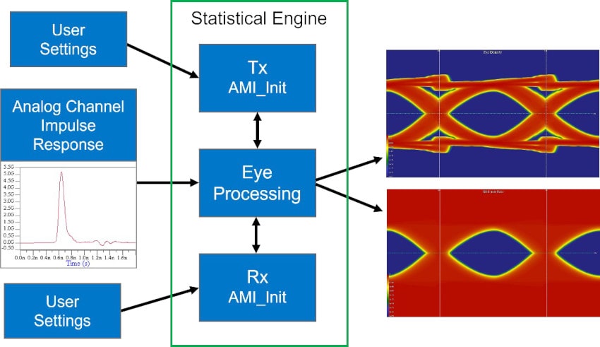
The result of this flow is a statistical eye digram that can be used to measure eye contours at different BER levels.
DDR5 Example Simulation
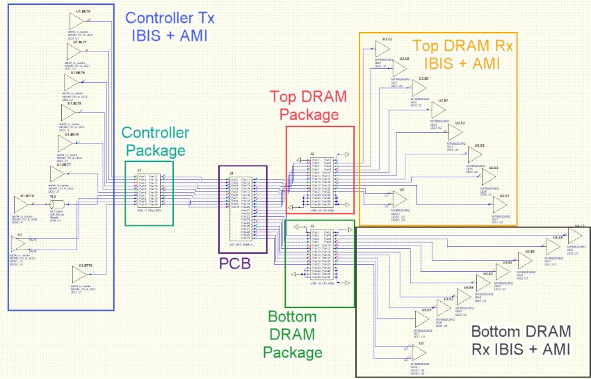
A DDR5 simulation was modeled in the HyperLynx LineSim tool, with the DQ and DQS IBIS-AMI models provided by Micron, and here’s the system schematic.
The EDA tool captures the waveform at specified clock times, where timing uncertainties within clock times are transferred into the resulting output eye diagram, reconstructing the voltage and timing margins before quantization by the slicer and its clock.
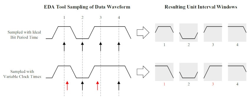
Both DQS and and DQ timing uncertainty impact the eye diagram similar to timing margin. Figure A shows jitter injected onto the DQ signal, and figure B has jitter injected onto the DQS signal. DQ (red) and DQS (green) jitter are shown together in figure C.
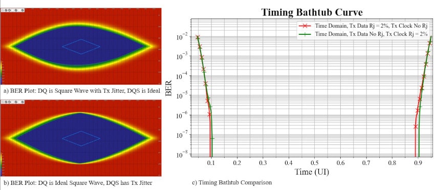
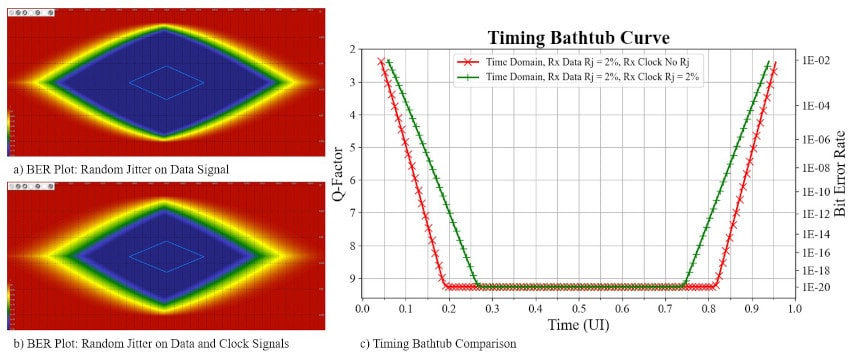
Sinusoidal jitter effects can even be modeled on the DQ signal and DQS signal in various combinations to see the BER and timing bathtub curve results. DDR5 has Rj, Dj and Tj measurements instead of period and cycle to cycle jitter measurements. The impact of Rx and Rj values on the BER plots can be simulated, along with the timing bathtub curves.
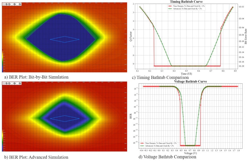
Going beyond Linear and Time-Invariant (LTI) modeling, the Multiple Edge Response (MER) technique uses a set of rising and falling edges. With a custom advanced IBIS-AMI flow it performs a statistical analysis on each MER edge, then superimposes the combined effect into an output eye diagram.
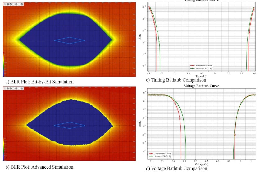
Adding Tx Rj values of 2% in the modeling shows even more realistic degraded BER plot results.
Summary
Signal Integrity effects dominate the design of a DDR5 system, so to get accurate results require detailed modeling of all the new physical effects. The IBS-AMI specification has been updated for Rx AMI models to use a forwarded clock. Micron showed how they used a clocked DDR5 simulation flow to model the new effects, including non-LTI effects, and achieving simulations with BER of 1e-16 and below.
Request and read the complete 25 page white paper online here.
Related Blogs
- DDR4 is a complex interface to verify — assistance needed!
- Standardization of Chiplet Models for Heterogeneous Integration
- Architectural Planning of 3D IC
- Verifications Horizons 2021, Now More Siemens
- Mainstream PCB Design Requires a Complete Tool Platform, Too
- Channel Operating Margin (COM) — A Standard for SI Analysis




Comments
There are no comments yet.
You must register or log in to view/post comments.