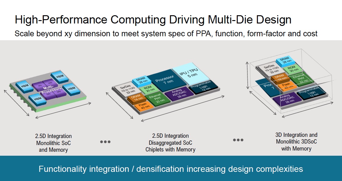
The move to true 3D IC, monolithic 3D SOC and 3D heterogeneous integration may require one of the most major design tool architecture overhauls since IC design tools were first developed. While we have been taking steps toward 3DIC with 2.5D designs with interposers, HBM, etc., the fundamental tools and flows remain intact in many cases. 3D IC designs that fully utilize and optimize silicon across all three dimensions offer big payoffs in performance, power and area (PPA) efficiency. This shift will also require IC tools and flows that work in a fully 3D manner.
Recently I had a chance to speak with Kenneth Larsen, director of product marketing at Synopsys, about the changes necessary to accommodate the move to 3D IC. Simply put, up until now the tools for 2D design and even those for 2.5D design have mostly worked in two-dimensional space. While there is a 3D component in all semiconductor designs, the operational paradigm has been to rely on 2D tools for design and layout accompanied by a lot of verification. It has been this way since the 1970s. With true 3D design, where several active chips are stacked together for the best solution, this will no longer be the case. New tools, like 3DIC Compiler Design Platform from Synopsys, that can drive PPA optimization across the cubic space of the 3D silicon stack will be needed.
There are many reasons to move to 3D IC design. In the case of systems-on-a-chip (SOCs), it means that instead of building a large monolithic die that has everything in one process technology, the optimal process technologies can be used for each specific subsystem while maintaining short interconnections and increasing density. The smaller subsystem dies from the disaggregated SOC can be selectively included in the final product. Even if separate processes are not needed, yield can increase with the use of small chip dies. Also, for SOCs that have different end-markets, SOCs can be disaggregated into so-called chiplets that can be reused and shared among several projects, amortizing cost so they can be shared over more designs.

Kenneth touched on the increased complexity that arises and how Synopsys 3DIC Compiler provides an environment that can handle the new workload. Bouncing between tools for digital implementation, custom implementation, packaging, analysis and test can create inconsistencies and lost transactions which exacerbate with increasing 3D design complexities. It is evident that similar to 2D IC design today, 3D IC design can also benefit from a unified flow environment that enables co-design of IP, silicon dies and package.
A 3D IC design will have through silicon vias (TSVs) and lateral die-to-die connections as signals move up and down in the Z-direction. There will be die-to-die connections with billions of bonds. According to Kenneth, the Synopsys 3DIC Compiler design management and data environment has been optimized for three-dimensional designs with more than 500 billion objects. Kenneth reviewed several approaches that are being used in the industry today, such as TSMC 3DFabric, Samsung X-Cube and Intel Foveros. The big takeaway was that there will be increasing flexibility in the way dies are connected within 3DICs and the software will need a native 3D representation to accommodate this.
The kinds of analysis and verification that are needed include multi-die thermal, signal and power integrity, static timing, as well as extraction and physical verification. The Synopsys 3DIC Compiler Design Platform integrates the leading golden sign-off tools from Synopsys and partners including Ansys via its 3D tool interoperability framework. The platform has been deployed into production use and has multiple tape-outs that have proven its value since its launch less than a year ago.
The leap from 2D to 3D has been a long time coming, but the days of hacking 2D applications for 2.5D designs are over. My conversation with Kenneth was informative and showed how heavily Synopsys has invested in creating a flow and environment that can support this new design approach. The case for 3D IC based design is compelling. More information on 3DIC Compiler from Synopsys is available on their website.
Also Read:
Die-to-Die Connections Crucial for SOCs built with Chiplets
Mars Perseverance Rover Features First Zoom Lens in Deep Space
Verification Management the Synopsys Way
Share this post via:


Comments
There are no comments yet.
You must register or log in to view/post comments.