The annual Siemens Digital Industries Software user group event was held virtually on May 26th, which made it easy to attend from my home office, although selecting from the list of speakers was a challenge, because they offered 475 sessions, wow. My focus is EDA, so I listened to Joseph Sawicki, the Executive Vice President, IC EDA Siemens Digital Industries Software. His on-demand session was entitled Silicon to Systems: From Vision to Reality. I first met Sawicki at Silicon Compilers in the 1980s, and have followed his career ever since then.
Digitalization
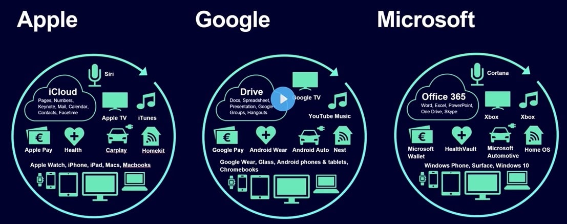
The most visible example of digitalization is seen in three big-name companies that are really systems companies, now with their own silicon products which enable them to offer a wide spectrum of business and personal products and services. These ecosystems are quite successful around the world.
Our smart phones are a common example of technology that is powered by silicon, connected to the cloud, running highly differentiated apps, creating multiple sources of revenue streams.
Smart Home
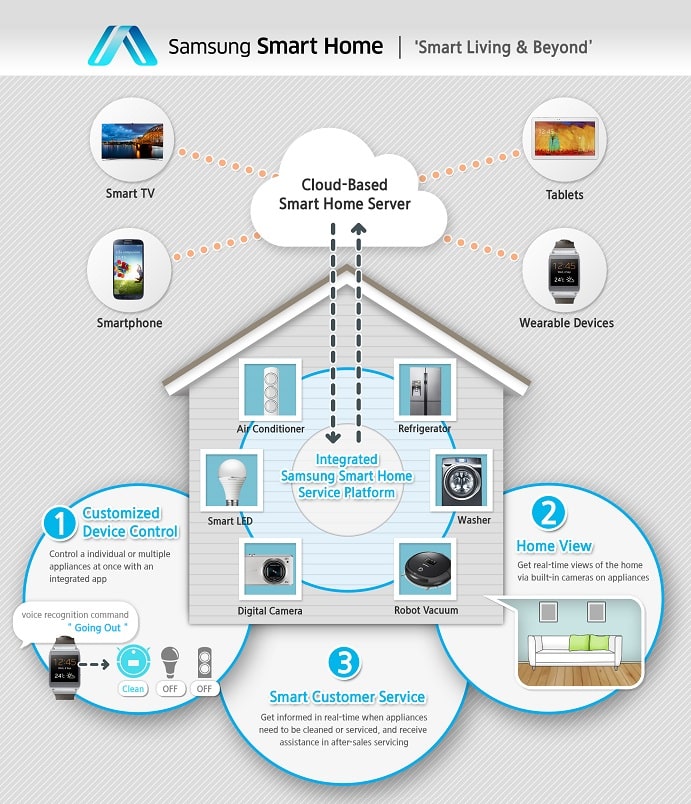
Consumer giant Samsung has a vision for the connected, smart home, only made possible with customized silicon chips, cloud connectivity and mobile apps.
Industrial IoT
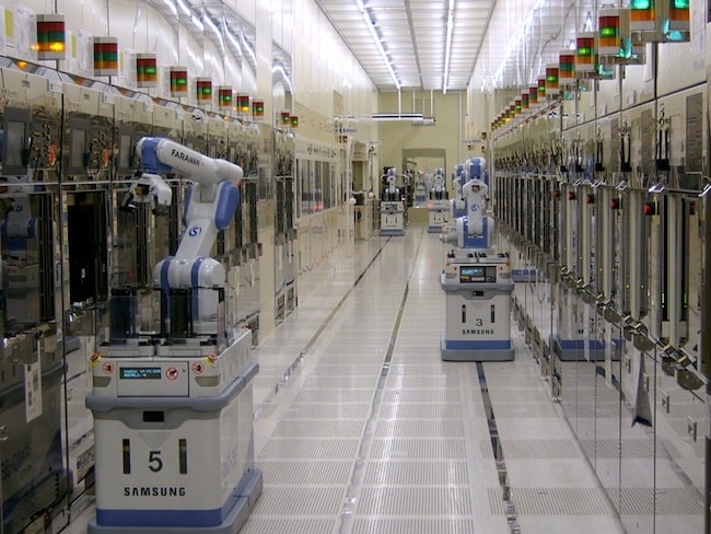
Factories are rapidly adopting new IoT technology and infrastructure to more efficiently run their business, even the semiconductor fabs are using robotics to help produce the next generation of silicon chips, where automated equipment with hundreds of sensors are now creating terabytes of data each month that require analytics to provide insight and help engineers make decisions.
Online Collaboration
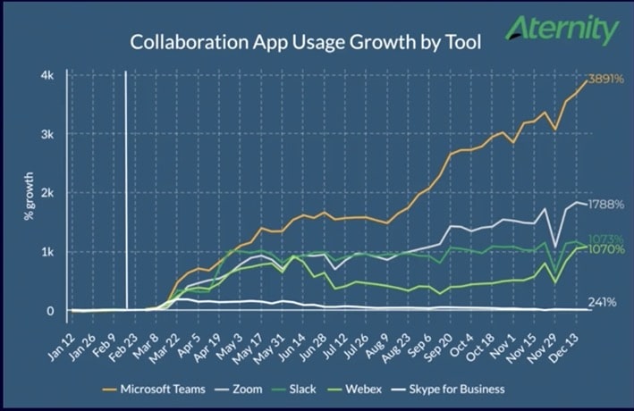
The pandemic has caused a rapid shift to online collaboration with platforms like: Microsoft Teams, Zoom, Slack, Webex and Skype. Both personal and business usage has skyrocketed for these platforms, all enabled by silicon, connectivity and apps. Before the pandemic it required us to travel around the globe in order to communicate with a wider audience as effectively.
Changes During COVID-19
KPMG did a survey to help quantify how the recent impact of COVID-19 has changed our workplace, and how digitalization is shaping that.
- 63% increased us of cloud and/or automation technologies
- 56% reduction in travel
- 55% permanent work from anywhere
- 24% revenue improvement for digital manufacturers over past 5 years
- 22% profitability improvement over 5 years for digital manufacturers
Siemens EDA will use a hybrid approach, where most employees can work from home and only come into the office a few days per week.
Semiconductor Growth Trends
Sensor and actuator annual shipments are now about 30 billion units, connected devices have a 10% CAGR, storage trends and data traffic are growing non-linearly, these are all causing semiconductor sales to grow. The history of silicon drivers over the years are:
- Industrial
- PC
- Cellphone
- Internet
- Smartphone
- Digitalization
Semiconductor revenues are about $500B today, with projections of a $1T market by 2030, where IBS has a 9.9% CAGR forecast to 2030.
Siemens EDA Vision
The response to all of this projected semiconductor growth then comes down to a vision with three themes:
- Technology Scaling – new nodes and 3D
- Design Scaling – using integration,
- System Scaling – validation and the digital twin
There are technology scaling roadmaps in place to 5nm, 3nm and even 2nm. Just over the past 8 years in smart phones the application processors used have seen tremendous change:
- Four nodes, 28nm to 5nm
- 36% smaller die size, 137mm2 to just 88mm2
- 12X increase in transistors, 1 billion to 11.8 billion
- 10X increase in CPU performance, 144 to 1,587 Geekbench single core
- 23X increase in GPU performance, 11.8 fps to 278.3 fps
Machine Learning Systems
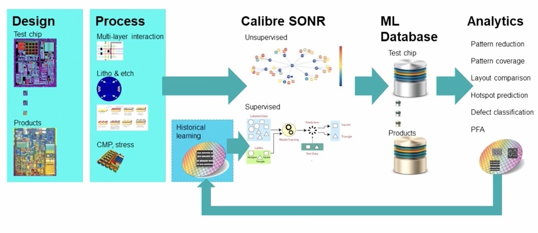
An example of applying machine learning to IC yield was shown with the Calibre SONR tool, used for predictive design and process insights to accelerate yield ramping.
Even failure data from post-silicon DFT tools can be fed back to yield engineers that help pinpoint where to improve the yield ramp for a new process or a new IC design.
Machine learning is also used in the Solido Variation Designer tool to help design, analyze and verify silicon IP in the presence of silicon variability. No more brute force Monte Carlo, all by using ML.
3D IC and Packaging
Siemens EDA has products used in four areas of 3D IC and packaging:
- Design – Xpedition Substrate Integrator
- Implementation – Xpedition Package Designer
- Verification – Calibre DRC & LVS, HyperLynx
- Analysis – Simcenter, HEEDS
Systems in package is another trend to watch in the journey from silicon to systems.
Design Scaling
High Level Synthesis (HLS) is a proven way to enable design scaling, like developing AI on the Edge systems with a better performance per watt per dollar. Using C+ and SystemC allows architectural exploration, creating more optimized silicon systems, for AI and video.
Digital place and route is part of physical IC implementation, and with the acquisition of Avatar, now Siemens EDA has a tool for billion-gate designs that can provide a faster time to design closure on advanced nodes.
System Scaling
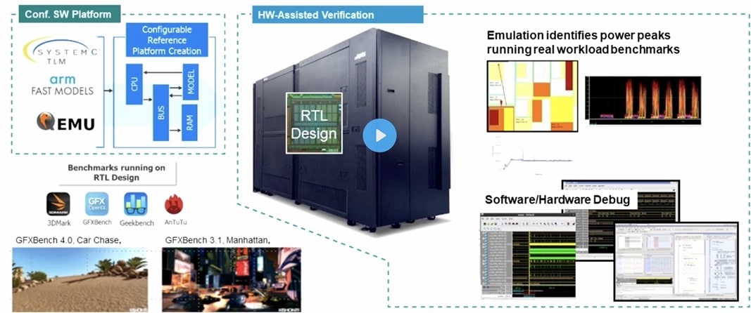
Model-based design has been going on with IC design for decades now, but new electronic systems have presented tougher validation challenges between hardware, software and applications. Hardware-assisted verification now allows you to boot the OS and run real apps, while monitoring power and looking for safety and security issues.
Virtualized Modeling of Systems
Over one year ago PAVE360 was announced, and it lets you model a real-world environment for automobiles, complete with sensors, actuators, and obstacles. This allows you to simulate billions of miles in a vehicle testing out your ADAS system, virtually.
Even a 5G ecosystem can be modeled for a complete smart factory, all before any radios or systems are even installed.
DFT
Extending DFT to include embedding analytical monitors, reporting about the health of a digital system is now possible. Improved security is enabled by embedded analytics.
Silicon to Systems
Siemens EDA is well positioned to deliver on these three themes of technology scaling, design scaling and system scaling as part of the silicon to systems trend. Joseph Sawicki made a compelling video presentation at the Realize LIVE event, and I look forward to the 2022 event being held in person.
Also Read:
Heterogeneous Chiplets Design and Integration
Siemens EDA Acquires an IP Validation Tool for standard cells, IO and Hard IP
Safety Architecture Verification, ISO 26262
Share this post via:



Comments
There are no comments yet.
You must register or log in to view/post comments.