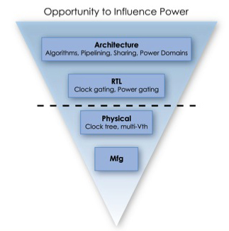
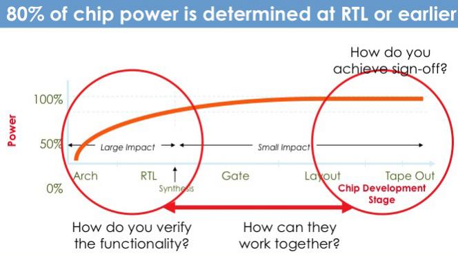
Major power reductions are possible by reducing power at the RTL and system levels, and not just at the gate and physical level. In fact, as is so often the case in design, changes can have much more impact when done at the higher level, even given that at that point in the design there is less accurate feedback about changes. Later the impact of a change is known much more accurately but the difference any change can make is smaller. In fact 80% of chip power is determined by the RTL level and above, and the maximum difference that can be made by clever synthesis and clock tree gating is 10-20%.

Power is, of course, a huge issue in SoC design. Not just for mobile and other battery powered devices, but also for tethered devices like servers and routers (a lot of the cost of a datacenter is cooling) or home DVRs and televisions (where fans are not acceptable). And all chips have potential thermal issues if the power is too high, from reliability to package cost.
There are many changes that can be made at the RTL level or above. Here are some of the most important ones:
- System architecture level
- SW-HW partitioning
- OS/firmware-level APIs for standby/sleep modes
- Single core vs Multi cores
- Bus and memory architecture
- Communication vs computation tradeoffs
- Micro-architecture level
- Frequency and voltage scaling
- Memory/register file banking
- Auto-inferencing of appropriate FIFOs and other communication channels
- RTL level
- Combinational clock gating
- Sequential clock gating
- Power gating
Below the RTL level the main optimization are multiple voltage domains, multiple threshold libraries (high performance on critical path, low power otherise) and clock network optimization.

On Tuesday November 19th Calypto is hosting a webinar. Abhishek Ranjan, who is a senior director of engineering, will present how to use Calypto’s HLS product Catapult along with the PowerPro RTL level power optimization tool, to reduce power at the architectural and RTL levels. The webinar is titled Techniques for Reducing Power at Various Levelsand will last about an hour. It starts at 11am Pacific Time. He will discuss dynamic voltage and frequency scaling (DVFS), power-gating, bus-data encoding, low power arithmetic architectures, memory-banking, sequential clock/memory gating and other micro-architectural techniques.
Details and registration are here. November 19th at 11am Pacific.
And a reminder about a Calypto webinar next week How to Maximize the Verification Benefit of High Level Synthesis with SystemC at 11am on Tuesday November 5th. Details and registration here. And for anyone from outside the US (or in Arizona!) we come off daylight savings time a couple of days before so make sure to log in at the correct time.
More articles by Paul McLellan…


Musk’s Orbital Compute Vision: TERAFAB and the End of the Terrestrial Data Center