

Grenoble is French city well-known within the Semiconductor industry to be one of the last location counting wafer fabs, not only in France but in fact in Europe. Back in the 70’s, under French government impulse, through the Commisariat à l’Energie Atomique (CEA) and the LETI subsidiary in charge of Electronic related research, the first wafer fab have been built in Grenoble, developing 5 micron MOS technologies. Almost 50 years later, there are still wafer fabs in Grenoble, processing wafers in 28 nm or even less. In the meantime, a complete ecosystem has emerged around CEA-LETI and ST-Microelectronics, counting companies like SOITEC (Silicon on Insulator wafer production) and several EDA start-up, most of them being hosted into a location called Minatec (please don’t ask me for the meaning of the acronym!). Atrenta is probably too old to be called a start-up, as the success of their flagship SPYGLASS product has put the company on the EDA forefront. When Atrenta has decided to create an Engineering team in charge of developing from scratch power dedicated EDA tools, they could have extended their Sri Lanka or India operations, they have started this new product line development in Grenoble instead.

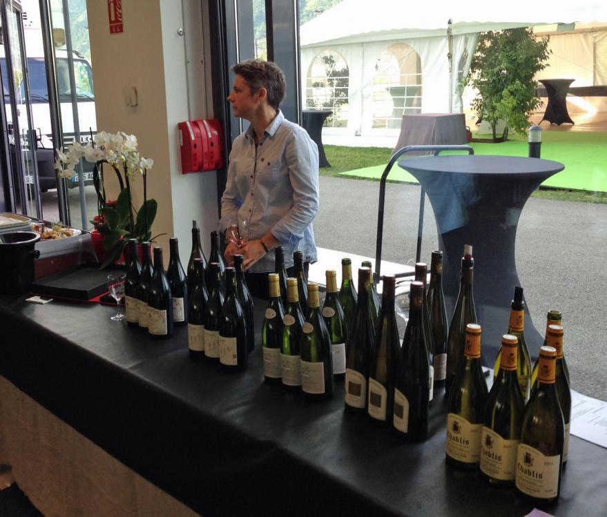
Last week, there was a party organized at Minatec, celebrating the two years anniversary of Atrenta implantation in Grenoble. If you consider that this party was a wine degustation, including:
- Chablis (Chardonnay) as a starter
- Crozes-Hermitage (Red wine, Syrah)
- Saint-Joseph (same)
- Condrieu (Vionnay)a wonderful white wine!
- To end with Cotes-Rotie, my preferred Cotes du Rhone…
How could I have escaped attending to such an event!
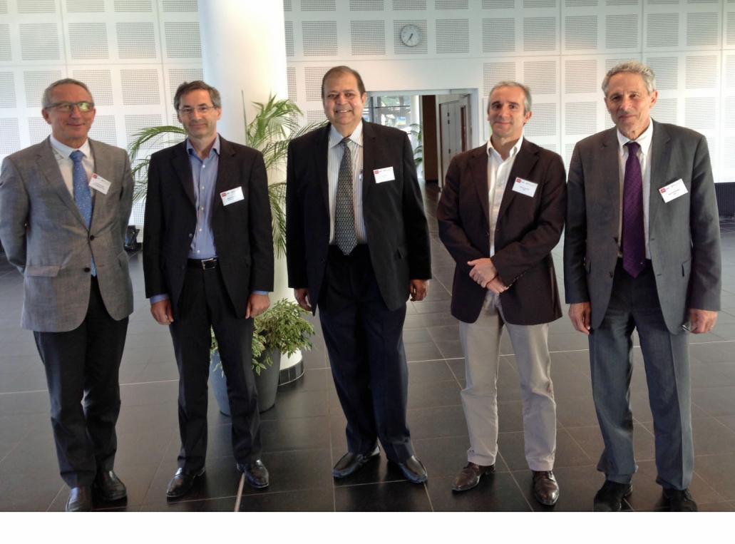
It was also an opportunity to meet with the complete Atrenta Grenoble team, pretty young engineers for the most, coming from all across Europe, as well as with managers from LETI and ST-Microelectronics, and obviously Atrenta, as Ajoy K. BOSE, Chairman and CEO was there, demonstrating that Atrenta is really committed to this Grenoble implantation! It was also an opportunity to hear a talk and meet with Philippe Magarshack, Executive VP at STM. In fact, I saw this name appearing in so many events and conferences that I thought it was a myth, but I can now guarantee that he is real, and very open to talk, especially if you speak about FDSOI (if you remember, I talked about FDSOI in Semiwiki a while ago)… Philippe is second from the left, when Ajoy is right on the middle on the above picture.
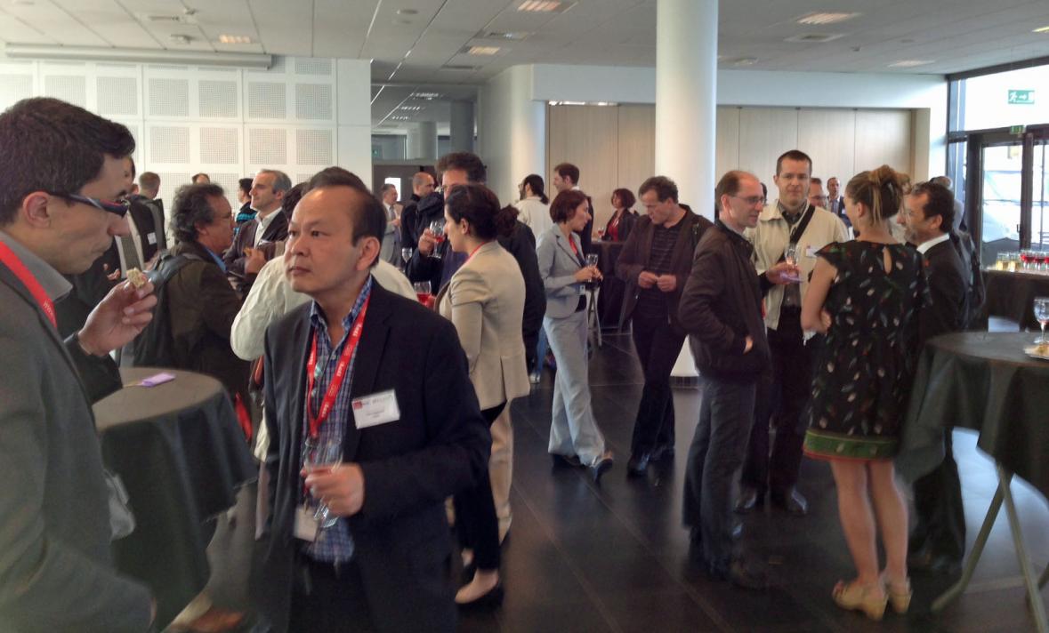
On the above picture, you can see that wine and networking are going well together!
Last point, Mike Gianfagna, Vice President of Corporate Marketing at Atrenta, commenting about the success of this Grenoble implantation, pointing the fact that it’s the first time, and first location in the world, where the conjunction of politic willingness, government backed program like MINATEC, semiconductor industry (STM) and advanced research (CEA-LETI) allow the emergence of such a R&D project that Atrenta has realized, and “simply works fine”.
Eric Esteve from IPNEST
lang: en_US


TSMC CoWoS versus Intel EMIB Semiconductor Packaging