You will never meet a more approachable CEO in the semiconductor ecosystem than Dr. Walden C. Rhines. The first time I met Wally was way back when I blogged for food and he invited me over for lunch. Even better, a year or two later I was having dinner with a friend at the DBL Tree in San Jose. Wally was waiting for his flight home so he joined us for a glass of wine and an impromptu industry discussion.
At the Mentor U2U conference today Wally did a replay of the presentation he did at the GlobalPress Electronics Summit which Paul McLellan blogged about HERE. Since I’m more of a foundry person let me comment on a different part of his presentation.
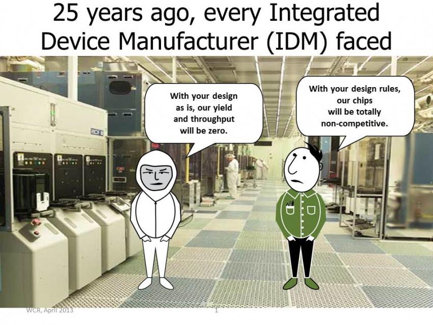
 Wally pointed out that when I started in this business almost 30 years ago semiconductor companies had their own fabs and could more accurately measure designs based on performance, power, area, AND manufacturability. With the emergence of independent semiconductor foundries this all changed. Manufacturing cost (yield) was a wedge between design and manufacturing. Fabless semiconductor companies emerged and pounded on the foundry doors begging for capacity for products that would have the best PPA (performance, power, area). The foundries wanted products that were manufacturable with high yield (low cost). It all came down to the choice of design rules: Should the design rule manuals (DRMs) be more accommodating to design with aggressive rules? Or should they be guard banded to allow for manufacturing variability?
First the foundries offered manufacturing centric DRMs with minimum design rules that had to be followed. As foundry competition emerged fabless companies had more choices and demanded more design oriented DRMs for better PPA. At 1.3m (from what I remember) the foundries compromised and introduced the concept of recommended design rules. The minimum rules were more design oriented (tight spacing) while the recommended (optional) rules were manufacturing oriented (larger spacing). Naturally the fabless designers did NOT use the recommended rules since they were not PPA focused, especially the ones purchasing good die versus wafers.

This arrangement broke at 40nm which resulted in an extended yield ramp and painful market delays. At 28nm recommended rules were done away with and more restrictive design rules were implemented. As a result, 28nm ramped in record time and will be the most successful process node we will ever see (my opinion). As the slides from my EDPS Keynote show, the more restrictive DRMs and DRC decks are, the larger and more complex they become.
This transition will continue to require better EDA tools for designers and fabs to manage this ongoing collaboration and resulting complexity. One example Wally used was the Calibre PERC product which we recently blogged about HERE. This transition will also require closer collaboration between the fabless companies, EDA companies, IP companies, and the foundries. CEO’s like Wally Rhines and conferences like U2U, DAC, Arm TechCon, and TSMC OIP are critical to our survival so I ask all executives in the fabless semiconductor ecosystem to please allocate budget and send your best people out to make sure we all thrive in the coming process nodes.
lang: en_US
Share this post via:


Comments
There are no comments yet.
You must register or log in to view/post comments.