You are currently viewing SemiWiki as a guest which gives you limited access to the site. To view blog comments and experience other SemiWiki features you must be a registered member. Registration is fast, simple, and absolutely free so please,
join our community today!
WP_Term Object
(
    [term_id] => 14433
    [name] => X-Subscriber
    [slug] => x-subscriber
    [term_group] => 0
    [term_taxonomy_id] => 14433
    [taxonomy] => category
    [description] =>
    [parent] => 0
    [count] => 0
    [filter] => raw
    [cat_ID] => 14433
    [category_count] => 0
    [category_description] =>
    [cat_name] => X-Subscriber
    [category_nicename] => x-subscriber
    [category_parent] => 0
    [is_post] =>
)
At Intel back in the late 1970’s we wanted to know what process corner each DRAM chip and wafer was trending at so we included a handful of test transistors in the scribe lines between the active die. Having test transistors meant that we could do a quick electrical test at wafer probe time to measure the P and N channel transistor… Read More
If you haven’t noticed, there has been a BIG influx of money into Artificial Intelligence (AI) technologies. Most recently, the Chinese government announced that AI is one of their top initiatives with a goal to catch up with the United States within 3 years and to be the world leader in AI by the year 2030. Horizon Robotics, founded… Read More
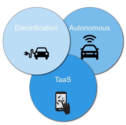
I come from a car-centric family where my father actually bought and sold over 300 vehicles in his lifetime, so automotive mega-trends pique my interest. A new conference called Semiconductors ISO 26262 held it’s first annual event last month, meeting in Munich with guest speakers from some impressive companies like: … Read More
2017 was a banner year for semiconductor sales as they topped $400B for the first time, an increase of some 20%, there is happiness in Silicon Valley, Taiwan, South Korea, and well, everywhere. With the foundries pushing to ever-smaller process dimensions and even going back to mature nodes and offering more variations that are… Read More
Two recently announced vulnerabilities in major processor platforms should remind us that bugs don’t organize themselves to appear only in domains we know how to test comprehensively. Both Meltdown and Spectre (the announced problems) are potential hardware system-level issues allowed by interactions between speculative… Read More
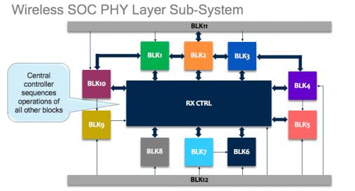
Semiconductor IP re-use is a huge part of the productivity gains in SoC designs, so instead of starting from a clean slate most chip engineers are re-using cells, blocks, modules and even sub-systems from previous designs in order to meet their schedule and stay competitive in the market place. But what happens when you intend to… Read More
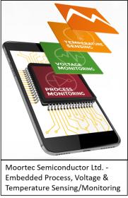
Six years ago I first interviewed Stephen Crosher, CEO and Co-founder of Moortecas they were in startup mode with some new semiconductor IP for temperature sensing, and earlier this month I attended their webinar all about embedded in-chip monitoring to get caught up with their technology and growing success. Ramsay Allen is … Read More
I attended Oski’s latest Decoding Formal event a couple of weeks ago and again enjoyed a largely customer-centric view of the problems to which they apply formal, and their experiences in making it work for them (with Oski help of course). From an admittedly limited sample of two of these events, I find them very representative of… Read More
I recently was introduced to a white paper written by John Stabenow, Director at Mentor, a Siemens Business, that gave an excellent overview of things to consider before launching into the design of an IoT edge project. John starts the paper with a quote from Pliny the Elder (A.D.23-A.D.79) who said, “The best plan is, as the common… Read More
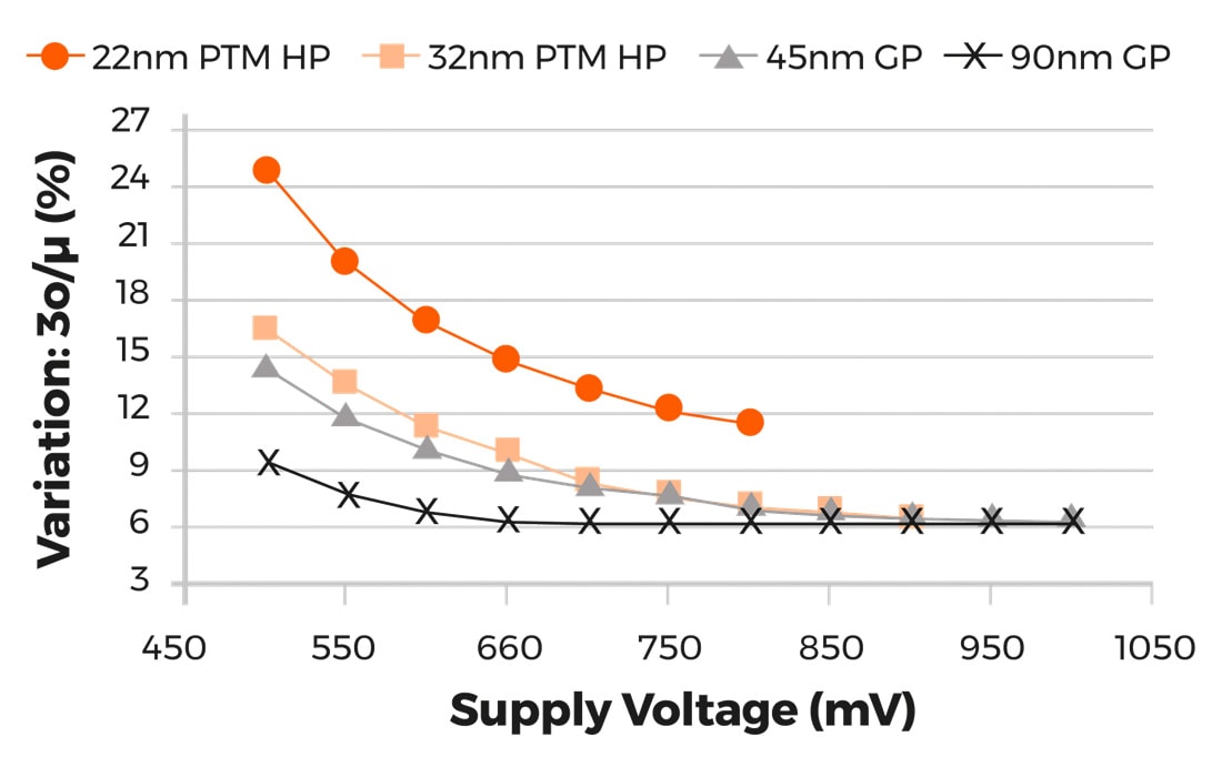
In a former life I was the GM of a business where we built specialized structures used for semiconductor process bring-up, characterization and monitoring. These monitoring structures were placed in wafer scribe-lines and were used to monitor key parameters during wafer processing. The structures provided feedback to automated… Read More