You are currently viewing SemiWiki as a guest which gives you limited access to the site. To view blog comments and experience other SemiWiki features you must be a registered member. Registration is fast, simple, and absolutely free so please,
join our community today!
WP_Term Object
(
    [term_id] => 14433
    [name] => X-Subscriber
    [slug] => x-subscriber
    [term_group] => 0
    [term_taxonomy_id] => 14433
    [taxonomy] => category
    [description] =>
    [parent] => 0
    [count] => 0
    [filter] => raw
    [cat_ID] => 14433
    [category_count] => 0
    [category_description] =>
    [cat_name] => X-Subscriber
    [category_nicename] => x-subscriber
    [category_parent] => 0
    [is_post] =>
)
ESD stands for electro-static discharge and deals with the fact that chips have to survive in an electrically hostile environment: people, testers, assembly equipment, shipping tubes. All of these can carry electric charge that has the “potential” (ho-ho) to damage the chip irreversibly. Historically this was… Read More
Kilopass was founded back in 2001 by Jack Peng, whose background was in FPGAs with his most recent position being manager of technology development at Actel (now part of Microsemi). The idea was to build a company making one-time-programmable (OTP) memories using anti-fuse technology. Fuses in home-wiring (OK, I know, we all … Read More
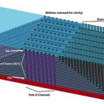
You may know that up until now NAND flash has been a planar technology. But just as with SoC processes where we have had to go vertical to FinFETs, NAND flash has reached the limitations of scaling in the 20nm nodes and is also going vertical. It is not just a lithography issue but there are also reliability and voltage scaling issues.… Read More
The long running legal action between the top two NVM IP companies is now finished after close to five years of lawyering. By the way, I write about this stuff in hopes of limiting the future earning power of lawyers that prey on our R&D budgets. This one is significant because Kilopass was not successful in a patent infringement… Read More
Verification in general suffers from a couple of fundamental problems. Availability of models and performance of different levels of representation.
The first problem, availability of models, is that you would like to start verification as soon as possible but all the representations are not ready early enough. Obviously … Read More
With today’s ArF based lithography using 193nm wavelength light, we are hard up against the limitations imposed by the Raleigh equation. Numerous clever things have been devised to maximize yield and reduce feature size. These include 2 beam lithography, multiple patterning, immersion litho processes to improve NA, thinner… Read More
At the end of last month during ISSCC there was a forum organized by the SOI Consortium. It took place in San Francisco at the Palace Hotel (which, if you have never been there, is famous for converting its old entryway for carriages into an amazing dining room, and for a bar with a huge painting by Maxfield Parrish of the Pied Piper valued… Read More
QuickLogic’s CTO Tim Saxe gave a keynote Getting a Grip on the Internet of Things at the IoT Summit last week.
He started by relating how things have changed over the last 3 years when he talks to customers.
- Three years ago it was sensor hubs in smartphones and the power budget was 3mW (so one day between re-charging, something
…
Read More
You have to love when a professional journalist leaks a story and cites a “source close to the acquisition.” News flash: Anyone “close” to the acquisition is under NDA which is a legally binding agreement, not very professional if you ask me. Bloggers however can write whatever they want but since I was actually “close” to … Read More
All chips these days have to worry about power. Indeed it is typically the top of the priority list of concerns, above performance and even area. Transistors are effectively fast and free, but you can’t have too many of them (at least turned on at once). The most obvious way to reduce power is to lower the supply voltage. This … Read More