Taiwan Semiconductor Manufacturing Company, the world’s largest dedicated semiconductor foundry, has transformed from a modest startup into a global technology powerhouse. Founded on February 21, 1987, by Morris Chang, a veteran of Texas Instruments, TSMC pioneered the “pure-play” foundry model. … Read More

AI-Driven DRC Productivity Optimization: Insights from Siemens EDA’s 2025 TSMC OIP Presentation
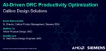
In the rapidly evolving semiconductor industry, Design Rule Checking (DRC) remains a critical bottleneck in chip design workflows. Siemens EDA’s presentation at the 2025 TSMC Open Innovation Platform Forum, titled “AI-Driven DRC Productivity Optimization,” showcases how artificial intelligence … Read More
Cerebras AI Inference Wins Demo of the Year Award at TSMC North America Technology Symposium
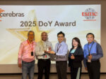
This is a clear reminder of how important the semiconductor ecosystem is and how closely TSMC works with customers. The TSMC Symposium started 30 years ago and I have been a part of it ever since. This event is attended by TSMC’s top customers and partners and is the #1 semiconductor networking event of the year, absolutely.… Read More
Accelerating SRAM Design Cycles: MediaTek’s Adoption of Siemens EDA’s Additive AI Technology at TSMC OIP 2025
In the competitive vertical of mobile System-on-Chip development, SRAM plays a pivotal role, occupying nearly 40% of chip area and directly impacting yield and performance. The presentation “Accelerating SRAM Design Cycles With Additive AI Technology,” co-delivered by Mohamed Atoua of Siemens EDA and Deepesh… Read More
TSMC Formally Sues Ex-SVP Over Alleged Transfer of Trade Secrets to Intel
The big semiconductor news this week is the legal action TSMC is taking against former Senior Vice President Wei-Jen Lo. This looks to be a serious game of 3D chess between CC Wei and Lip-Bu Tan so it is worth a look. I got this notice in my inbox early Tuesday morning:
Immediately following, there was an interesting discussion on SemiWiki… Read More
TSMC Kumamoto: Pioneering Japan’s Semiconductor Revival

In the lush landscapes of Kumamoto Prefecture, on Japan’s Kyushu Island, TSMC is etching a new chapter in global chip production. The TSMC Kumamoto facility, operationalized through its wholly-owned subsidiary Japan Advanced Semiconductor Manufacturing (JASM), represents the Taiwanese giant’s bold foray… Read More
Memory Matters: The State of Embedded NVM (eNVM) 2025

Make a difference and take this short survey. It asks about your experience with embedded non-volatile memory technologies. The survey is anonymous, and the results will be shared in aggregate to help the industry better understand trends: 2025 Embedded Non-Volatile Memory Survey.
We are now in the AI era where data is the lifeblood… Read More
AI-Driven DRC Productivity Optimization: Revolutionizing Semiconductor Design
The semiconductor industry is undergoing a transformative shift with the integration of AI into DRC workflows, as showcased in the Siemens EDA presentation at the 2025 TSMC OIP. Titled “AI-Driven DRC Productivity Optimization,” this initiative, led by Siemens EDA’s David Abercrombie alongside AMD’s… Read More
Exploring TSMC’s OIP Ecosystem Benefits

Now that the dust has settled let’s talk more about TSMC’s Open Innovation Platform. Launched in 2008, OIP represents a groundbreaking collaborative model in the semiconductor industry. Unlike IDMs that controlled the entire supply chain, OIP fosters an “open horizontal” ecosystem uniting TSMC… Read More
Breaking the Thermal Wall: TSMC Demonstrates Direct-to-Silicon Liquid Cooling on CoWoS®
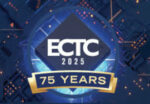
In a landmark presentation at the 2025 IEEE Electronic Components and Technology Conference (ECTC), TSMC unveiled a groundbreaking advancement in thermal management: Direct-to-Silicon Liquid Cooling integrated directly onto its CoWoS® platform. This innovation, detailed in the paper “Direct-to-Silicon Liquid… Read More