You are currently viewing SemiWiki as a guest which gives you limited access to the site. To view blog comments and experience other SemiWiki features you must be a registered member. Registration is fast, simple, and absolutely free so please,
join our community today!
WP_Term Object
(
    [term_id] => 386
    [name] => Semiconductor Services
    [slug] => semiconductor-services
    [term_group] => 0
    [term_taxonomy_id] => 386
    [taxonomy] => category
    [description] =>
    [parent] => 0
    [count] => 1226
    [filter] => raw
    [cat_ID] => 386
    [category_count] => 1226
    [category_description] =>
    [cat_name] => Semiconductor Services
    [category_nicename] => semiconductor-services
    [category_parent] => 0
    [is_post] =>
)
The Linley Group is an industry-leading source for independent technology analysis of semiconductors for networking, communications, mobile, and data-center applications. Their Microprocessor Report is widely read as a source of un-biased, no-nonsense analysis of technologies and trends. So, when they dig into something… Read More
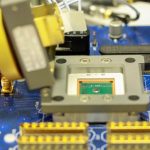
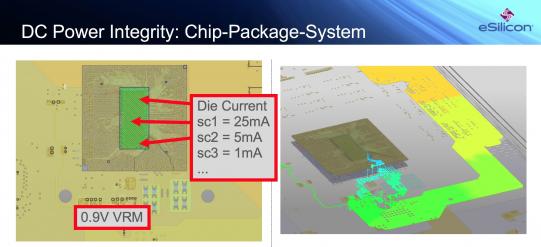
While I missed ANSYS (and indeed everyone else) at DAC this year, I was able to attend the ANSYS Innovation Conference last week at the Santa Clara Convention Center. My primary purpose for being there was to listen to a talk by eSilicon which I’ll get to shortly, but before that I sat through a very interesting presentation on the growing… Read More
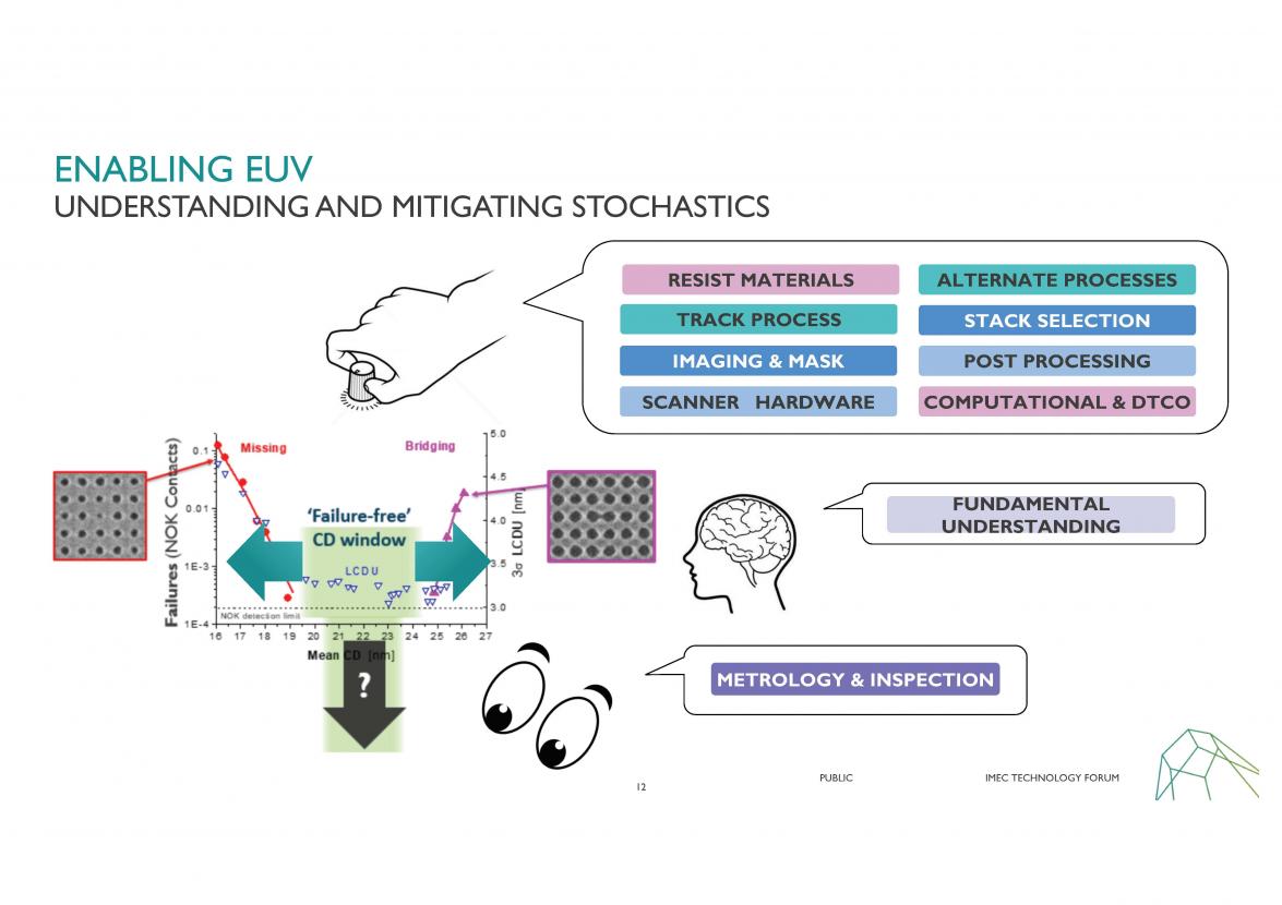
At SEMICON West I attended the imec technology forum, multiple Tech Spot presentations and conducted a number of interviews relevant to advanced lithography and EUV. In this article I will summarize what I learned plus make some comments on the outlook for EUV.… Read More
While writing “Mobile Unleashed: The Origin and Evolution of ARM Processors In Our Devices” it was very clear to me that ARM was an IP phenomenon that I did not believe would ever be repeated. Clearly I was wrong as we now have RISC-V with an incredible adoption rate, a full fledged ecosystem, and top tier implementers… Read More
I think most of us can attest that changing jobs is one of the most stressful decisions we make, as our careers progress. Making a job change is rarely an easy decision, though admittedly, so wonderful when it accomplishes your career and life goals. Having the right, well thought out expectations is the best way to ensure success,… Read More
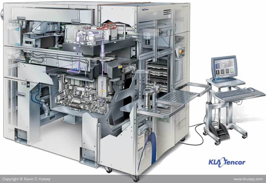
KLAC put up a great quarter coming in at revenues of $1.07B and EPS of $2.22. Guidance is for $1.03B to $1.1B with EPS of $2 to $2.32. Both reported and guided were at the high end of the range and above consensus. We had suggested in our preview notes that KLAC would be the least impacted of the big three (AMAT, LRCX & KLAC) semi equipment… Read More
AI is revolutionizing and transforming virtually every industry in the digital world. Advances in computing power and deep learning have enabled AI to reach a tipping point toward major disruption and rapid advancement. However, these applications require much higher performance and bandwidth requiring new kinds of IP and… Read More
Lam Research (LRCX) reported a great June quarter coming in at $3.126B in revenues and $5.31 in EPS easily beating the street’s $3.06B and EPS of $4.94. However no one will care as guidance for the September quarter is for $2.3B in revs and EPS of $3.20, way, well below the already downward revised estimates of $2.77B and $3.88.… Read More
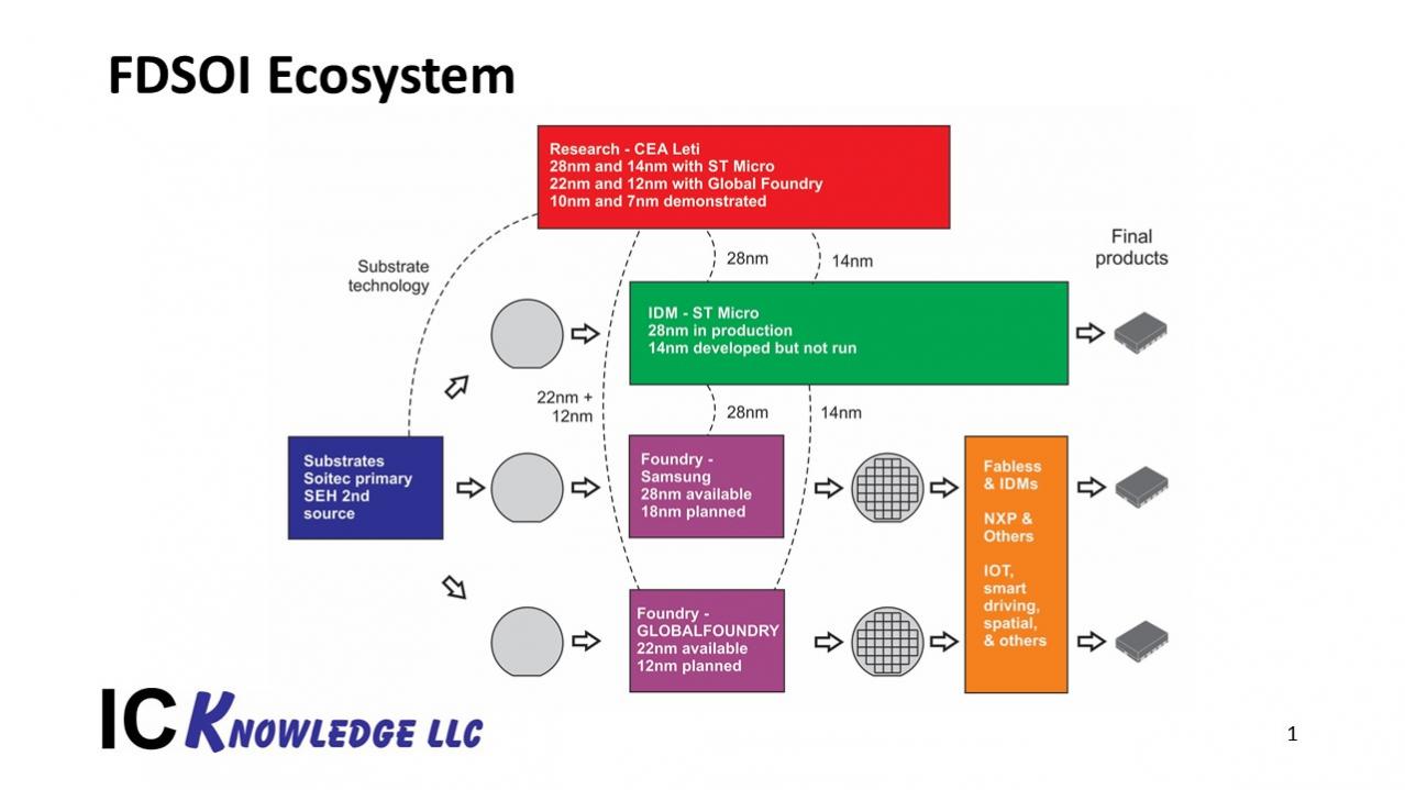
FDSOI is gaining traction in the market place. At their foundry forum in May, Samsung announced they have 17 FDSOI products in high volume manufacturing (you can read Tom Dilliger’s write up of the Samsung Foundry Forum here). At SEMICON West in July, GLOBALFOUNDRIES (GF) announced FDSOI design wins worth $2 billion dollars in … Read More
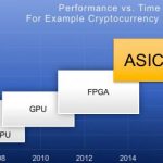
There is a well-known progression in the efficiency of different platforms for certain targeted applications such as AI, as measured by performance and performance/Watt. The progression is determined by how much of the application can be run with specialized hardware-assist rather than software, since hardware can be faster… Read More


TSMC CoWoS versus Intel EMIB Semiconductor Packaging