You are currently viewing SemiWiki as a guest which gives you limited access to the site. To view blog comments and experience other SemiWiki features you must be a registered member. Registration is fast, simple, and absolutely free so please, join our community today!
I was recently updating an analysis I did last year that looked at EUV system supply and demand, while doing this I started thinking about Intel and their Fab portfolio.
If you look at Intel’s history as a microprocessor manufacturer, they are typically ramping up their newest process node (n), in volume production… Read More
Now that Intel is back in the foundry business, and with the Tower Semiconductor acquisition they are definitely back in the foundry business, Samsung will be the biggest foundry loser here.
You can break the IDM foundry business into two parts: First, and foremost, the NOT TSMC Business. Second is the the Better PPA (Power/Performance,… Read More
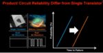
Intel recently released an exceptional video providing an insightful chronology of MOS transistor technology. Evolution of Transistor Innovation is a five-minute audiovisual adventure, spanning 50 years of Moore’s Law. Some of the highlights are summarized below, with a few screen shot captures – the full video is definitely… Read More
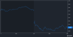
Intel’s big investor day was anything but big. The stock reacted poorly, down 5% on a day that was a widespread sell-off anyways.
I want to briefly summarize what matters for the stock. There was very little incremental news to the technology roadmap, and the financial outlook was underwhelming, to say the least.
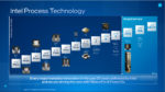
Last Thursday Intel held their investors meeting, in this write up I wanted to focus on my areas of coverage/expertise, process technology and manufacturing.
Technology Development presented by Ann Kelleher
Last year Intel presented their Intel Accelerated plan and, in this meeting, we got a review of where Intel stands on that… Read More
-Intel jumpstarts foundry model with Tower semi buy @$54B Gets complementary tech to round out offerings
-Approval based on satisfying China’s needs as well
-Margin concerns overblown- Will it be allowed to flourish?
Intel pays up to get foundry and technology….
Intel announced a $5.4B acquisition of Tower Semiconductor… Read More
Exciting times for the semiconductor industry! Last week Intel announced a billion dollar fund to build a foundry ecosystem and today Intel announced they are acquiring foundry Tower Semiconductor for $5.6 billion dollars, WOW! Some people doubted Intel’s commitment to the foundry market this time. I think we can now put that… Read More
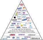
The last year has seen a ton written about the semiconductor industry: chip shortages, the CHIPS Act, our dependence on Taiwan and TSMC, China, etc.
But despite all this talk about chips and semiconductors, few understand how the industry is structured. I’ve found the best way to understand something complicated is to diagram… Read More
Kinam Kim is a longtime Samsung technologist who has published many excellent articles over the years. He is now the Chairman of Samsung Electronics, and he gave a very interesting keynote address at IEDM.
He began with some general observations:
The world is experiencing a transformation powered by semiconductors that has been… Read More

Enhancing Multi-Domain System Simulation with FMI Co-Simulation