You are currently viewing SemiWiki as a guest which gives you limited access to the site. To view blog comments and experience other SemiWiki features you must be a registered member. Registration is fast, simple, and absolutely free so please,
join our community today!
WP_Term Object
(
    [term_id] => 158
    [name] => Foundries
    [slug] => semiconductor-manufacturers
    [term_group] => 0
    [term_taxonomy_id] => 158
    [taxonomy] => category
    [description] =>
    [parent] => 0
    [count] => 1364
    [filter] => raw
    [cat_ID] => 158
    [category_count] => 1364
    [category_description] =>
    [cat_name] => Foundries
    [category_nicename] => semiconductor-manufacturers
    [category_parent] => 0
    [is_post] =>
)
What’s new with Glofo? Quite a bit actually. It was interesting to see a Made in America: Global Companies Expand in U.S. Towns segment on semiconductors! Give it a look, I enjoyed it. It’s an election year, jobs are key to any election, so it did not surprise me to see President Obama making the rounds:… Read More
While the debate rages on about 28nm yield at foundry juggernaut TSMC, on Monday I attended a webinar on 20nm IC design hosted by TSMC and Synopsys. Double Patterning Technology (DPT) becomes a requirement for several layers of your 20nm IC design which then impact many of your EDA tools and methodology.… Read More
There is an interesting discussion in the SemiWiki forum in response to the EETimes article: Intel exec says fabless model ‘collapsing’. Definitely an interesting debate, one worth our time since the advertising click hungry industry pundits will certainly jump all over it. Clearly I’m biased since I helped build… Read More
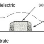
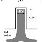
The previous post in this series provided an overview of FinFET devices. This article will briefly cover FinFET fabrication.
The major process steps in fabricating silicon fins are shown in Figures 1 through 3. The step that defines the fin thickness uses Sidewall Image Transfer (SIT). Low-pressure chemical vapor (isotropic)… Read More
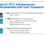
In every Intel product announcement and PR event, there are hours of behind the scenes meetings to discuss what they should introduce, what are the messages and what are the effects on the marketplace to maximize the impact of the moment. The Ivy Bridge product release speaks volumes of what they want to accomplish over the coming… Read More
TSMC just finished theQ1 conference call. I will let the experts haggle over the wording of the financial analysis, but the big news is that TSMC 28nm Q1 revenue was 5%, beating my guess of 4%. So all of you who bet against TSMC 28nm it’s time to pay up! Coincidentally, I’m in Las Vegas where the term deadbeat is taken literally!
Per my … Read More
For a long time Cisco had a very high end product whose official internal name during its years of development was HFR, which stood for Huge F***ing Router (the marketing department insisted it stood for ‘fast’). Eventually it got given a product number, CRS-1, but not before I’d read an article about it in the… Read More
The biggest news out of the TSMC Symposium last week was the 20nm update. Lots of debate and speculation, just why is TSMC releasing one version of 20nm (20nm SoC) versus multiple versions like in 40nm (LP, G, LPG) and 28nm (HP, HPM, HPL, LP)? Here are my thoughts, I would also be interested in your feedback in the comment section. This… Read More
First the good news: 4G LTE design in activity is off the charts as OEMs building smartphones, tablets and Ultrabooks are buying into the capability for product rollouts that will occur starting in September. Now the bad news: there’s not enough to go around until probably well into 2013. For a Company sitting on over $26B in cash,… Read More
This is the first of a multi-part series, to introduce FinFET technology to SemiWiki readers. These articles will highlight the technology’s key characteristics, and describe some of the advantages, disadvantages, and challenges associated with this transition. Topics in this series will include FinFET fabrication,… Read More


Chemical Origins of Environmental Modifications to MOR Lithographic Chemistry