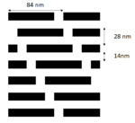
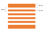
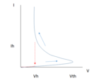
The overwhelming majority of transistors produced in the world are used in memory cells, either as the memory itself (Flash, SRAM), or as the access device (DRAM). Yet, it is not necessary to have a transistor in every memory cell. In 2015, 3D XPoint, the first major product based on transistor-less memory cells, was announced [1].
Feature-Selective Etching in SAQP for Sub-20 nm Patterning
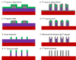
Self-aligned quadruple patterning (SAQP) is the most widely available technology used for patterning feature pitches less than 38 nm, with a projected capability to reach 19 nm pitch. It is actually an integration of multiple process steps, already being used to pattern the fins of FinFETs [1] and 1X DRAM [2]. These steps, shown… Read More
Contact Resistance: The Silent Device Scaling Barrier
Moore’s Law has been about device density, specifically transistor density, increasing every certain number of years. Although cost is the most easily grasped advantage, there are two other benefits: higher performance (speed) and reduced power. When these benefits are compromised, they can also pose a scaling limitation.
The Uncertain Phase Shifts of EUV Masks
EUV (Extreme UltraViolet) lithography has received attention within the semiconductor industry since its development inception in 1997 with the formation of the EUV LLC [1], and more recently, since the 7nm node began, with limited use by Samsung and TSMC being touted as key advantages [2, 3]. As with any key critical technology,
MOSFET Gate Length Scaling Limit at Reduced Threshold Voltages
As transistor dimensions shrink to follow Moore’s Law, the functionality of the gate used to switch on or off the current is actually being degraded by the short channel effect (SCE) [1-5]. Moreover, the simultaneous reduction of voltage aggravates the degradation, as will be discussed below.
A Practical Lower Limit of… Read More
Reliable Line Cutting for Spacer-based Patterning
Spacer-defined patterning is an expected requirement for advanced semiconductor patterning nodes with feature sizes of 25 nm or less. As the required gaps between features go well below the lithography tool’s resolution limit, the use of cut exposures to separate features is used more often, especially in chips produced… Read More
Lithography Resolution Limits: Line End Gaps
In a previous article [1], the Rayleigh criterion was mentioned as the resolution limit for the distance between two features. On the other hand, in a following article [2], the minimum pitch was mentioned for the resolution limit for arrayed features. In this article, we reconcile the two by considering gaps between arrayed features,… Read More
ASML A Scenario More Lumpy While Demand and Tech Remain Solid Despite Covid Delays
Covid issues create “lumpy” quarters due to delays
Orders & demand remain solid and strong
2020 Year financials intact so far but ignore Qtrs
Taking prudent actions- no buybacks or guidance
As expected, Covid impacts both shipments & supply chain, ignore the near term lumpiness…
ASML reported revenues… Read More
SPIE 2020 – ASML EUV and Inspection Update
I couldn’t attend the SPIE Advanced Lithography Conference this year for personal reasons, but last week Mike Lercel of ASML was nice enough to walk me through the major ASML presentations from the conference.
Introduction
In late 2018, Samsung and TSMC introduced 7nm foundry logic processes with 5 to 7 EUV layers, throughout … Read More
Lithography Resolution Limits – Arrayed Features
State-of-the-art chips will always include some portions which are memory arrays, which also happen to be the densest portions of the chip. Arrayed features are the main targets for lithography evaluation, as the feature pitch is well-defined, and is directly linked to the cost scaling (more features per wafer) from generation… Read More
Facing the Quantum Nature of EUV Lithography