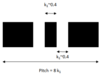
You are currently viewing SemiWiki as a guest which gives you limited access to the site. To view blog comments and experience other SemiWiki features you must be a registered member. Registration is fast, simple, and absolutely free so please,
join our community today!
WP_Term Object
(
[term_id] => 16126
[name] => Lithography
[slug] => lithography
[term_group] => 0
[term_taxonomy_id] => 16126
[taxonomy] => category
[description] =>
[parent] => 0
[count] => 166
[filter] => raw
[cat_ID] => 16126
[category_count] => 166
[category_description] =>
[cat_name] => Lithography
[category_nicename] => lithography
[category_parent] => 0
[is_post] =>
)
As transistor dimensions shrink to follow Moore’s Law, the functionality of the gate used to switch on or off the current is actually being degraded by the short channel effect (SCE) [1-5]. Moreover, the simultaneous reduction of voltage aggravates the degradation, as will be discussed below.
A Practical Lower Limit of… Read More
Spacer-defined patterning is an expected requirement for advanced semiconductor patterning nodes with feature sizes of 25 nm or less. As the required gaps between features go well below the lithography tool’s resolution limit, the use of cut exposures to separate features is used more often, especially in chips produced… Read More
In a previous article [1], the Rayleigh criterion was mentioned as the resolution limit for the distance between two features. On the other hand, in a following article [2], the minimum pitch was mentioned for the resolution limit for arrayed features. In this article, we reconcile the two by considering gaps between arrayed features,… Read More
Covid issues create “lumpy” quarters due to delays
Orders & demand remain solid and strong
2020 Year financials intact so far but ignore Qtrs
Taking prudent actions- no buybacks or guidance
As expected, Covid impacts both shipments & supply chain, ignore the near term lumpiness…
ASML reported revenues… Read More
I couldn’t attend the SPIE Advanced Lithography Conference this year for personal reasons, but last week Mike Lercel of ASML was nice enough to walk me through the major ASML presentations from the conference.
Introduction
In late 2018, Samsung and TSMC introduced 7nm foundry logic processes with 5 to 7 EUV layers, throughout … Read More
State-of-the-art chips will always include some portions which are memory arrays, which also happen to be the densest portions of the chip. Arrayed features are the main targets for lithography evaluation, as the feature pitch is well-defined, and is directly linked to the cost scaling (more features per wafer) from generation… Read More
As any semiconductor process advances to the next generation or “node”, a sticky point is how to achieve the required higher resolution. As noted in another article [1], multipatterning (the required use of repeated patterning steps for a particular feature) has been practiced already for many years, and many have… Read More
EUV lithography is widely perceived to be the obvious choice to replace DUV lithography due to the shorter wavelength(s) used. However, there’s a devil in the details, or a catch if you will.
Electrons have the last word
The resist exposure is completed by the release of electrons following the absorption of the EUV photon.… Read More
Extreme ultraviolet (EUV) lithography targets sub-20 nm resolution using a wavelength range of ~13.3-13.7 nm (with some light including DUV outside this band as well) and a reflective ring-field optics system. ASML has been refining the EUV tool platform, starting with the NXE:3300B, the very first platform with a numerical
…
Read More
I wasn’t able to attend the SPIE Advanced Lithography Conference this year for personal reasons, but Applied Materials was kind enough to set up a phone briefing for me with Regina Freed to discuss their Materials-Enabled Patterning announcement.
At IEDM Applied Materials (AMAT) tried to put together a panel across the entire… Read More
CHIPS Act dies because employees are fired – NIST CHIPS people are probationary