You are currently viewing SemiWiki as a guest which gives you limited access to the site. To view blog comments and experience other SemiWiki features you must be a registered member. Registration is fast, simple, and absolutely free so please,
join our community today!
WP_Term Object
(
    [term_id] => 50
    [name] => Events
    [slug] => events
    [term_group] => 0
    [term_taxonomy_id] => 50
    [taxonomy] => category
    [description] =>
    [parent] => 0
    [count] => 1522
    [filter] => raw
    [cat_ID] => 50
    [category_count] => 1522
    [category_description] =>
    [cat_name] => Events
    [category_nicename] => events
    [category_parent] => 0
    [is_post] =>
)
The live events I have attended thus far this year have been very good. As much as I liked the virtual events, attending in the comfort of my home or sailboat, it is great to be live and networking inside the semiconductor ecosystem, absolutely.
Ansys has been a great supporter of the Design Automation Conference but this year they … Read More
The VLSI Symposium on Technology & Circuits will be held in Hawaii from June 12th to June 17th. You can register for the conference here.
The tip sheet for the conference has been released and one thing that caught my eye is some data from the Intel 4 paper that Intel will be presenting at the conference.
Intel’s old roadmap had 14nm,… Read More
I attended the annual user group meeting called User2User in Santa Clara this year, hosted by Siemens EDA, with 51 presentations by customers in 11 tracks, and keynotes during each lunch hour from semiconductor executives. Joseph Sawicki, Executive VP, IC Segment, at Siemens EDA presented on a Tuesday, along with Prashant Varshney,… Read More
With the TSMC Technical Symposium coming next month there is quite a bit of excitement inside the fabless semiconductor ecosystem. Not only will TSMC give an update on N3, we should also hear details of the upcoming N2 process.
Hopefully TSMC will again share the number of tape-outs confirmed for their latest process node. Given… Read More
Are 112G PAM4 channels in one of your current or future designs? If you’re focusing on advanced products, the answer is likely YES. Design of these channels is quite challenging. Silicon design, SerDes, PCB traces, and interconnect all need to be balanced to achieve success. As they say, getting there is half the fun. An upcoming… Read More
The tremendous increase in global data traffic over the past decade shows no sign of abating. Indeed, the applications for all facets of data communications are expanding, from 5G (and soon, 6G) wireless communications to metropolitan area networks serving autonomous vehicles to broader deployment of machine learning algorithms. … Read More
Earlier this year semiconductor oracle Malcom Penn did his 2022 forecast which I covered here: Are We Headed for a Semiconductor Crash? The big difference with this update is the black economic clouds that are looming which may again highlight Malcolm’s forecasting prowess. I spent an hour with Malcolm and company on his Zoom cast… Read More
Andrew Levy and I both worked at Intel and Opmaxx, and I knew that he was now working at Alphacore, an IP company specializing in mixed-signal, RF, imaging and rad-hard applications. I was curious what Alphacore was up to, so at the IP-SoC Silicon Valley 2022 event I watched the ADC presentation from Ken Potts, COO of Alphacore. Mr.… Read More
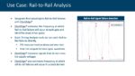
Proper clock functionality and performance are essential for SoC operation. Static timing analysis (STA) tools have served well for verifying clocks, yet with new advanced process nodes, lower operating voltages, higher clock speeds and higher reliability requirements, STA tools alone can’t perform the kinds of analysis… Read More
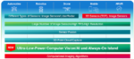
It’s popular to use DSP chips for vision processing in diverse applications like ADAS, security cameras and AR. Tensilica has been designing DSP chips and IP since 1997, and their technology was successful enough that Cadence acquired Tensilica back in 2013. At the IP-SoC Silicon Valley 2022 event in April I had the pleasure… Read More


Musk’s Orbital Compute Vision: TERAFAB and the End of the Terrestrial Data Center