You are currently viewing SemiWiki as a guest which gives you limited access to the site. To view blog comments and experience other SemiWiki features you must be a registered member. Registration is fast, simple, and absolutely free so please,
join our community today!
WP_Term Object
(
    [term_id] => 50
    [name] => Events
    [slug] => events
    [term_group] => 0
    [term_taxonomy_id] => 50
    [taxonomy] => category
    [description] =>
    [parent] => 0
    [count] => 1522
    [filter] => raw
    [cat_ID] => 50
    [category_count] => 1522
    [category_description] =>
    [cat_name] => Events
    [category_nicename] => events
    [category_parent] => 0
    [is_post] =>
)
At the VLSI Technology Symposium Imec presented on Buried Power Rails (BPR) and Backside Power Delivery (BSPD) in a paper entitled: “Scaled FinFETs Connected by Using Both Wafer Sides for Routing via Buried Power Rails”. I recently had a chance to interview one of the authors, Naoto Horiguchi about the work. I have interviewed … Read More
TSMC recently held their annual Technology Symposium in Santa Clara, CA. The presentations provide a comprehensive overview of their technology status and upcoming roadmap, covering all facets of the process technology and advanced packaging development. This article will summarize the highlights of the advanced packaging… Read More
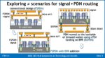
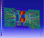
Semiconductor manufacturers are under constantly increasing and intense pressure to accelerate innovative new chip designs to market faster than ever in smaller package sizes while assuring signal integrity and reducing power consumption. Three-dimensional integrated circuits (3D-ICs) promise to answer all these demands… Read More
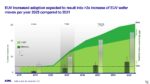
At the 2022 SPIE Advanced Lithography Conference, ASML presented an update on EUV. I recently had a chance to go over the presentations with Mike Lercel of ASML. The following is a summary of our discussions.
0.33 NA
The 0.33 NA EUV systems are the production workhorse systems for leading edge lithography today. 0.33 NA systems are… Read More
TSMC recently held their annual Technology Symposium in Santa Clara, CA. The presentations provided a comprehensive overview of their status and upcoming roadmap, covering all facets of process technology and advanced packaging development. This article will summarize the highlights of the process technology updates… Read More
The TSMC Technical Symposium is today so I wanted to give you a brief summary of what was presented. Tom Dillinger will do a more technical review as he has done in the past. I don’t want to steal his thunder but here is what I think are the key takeaways. First a brief history lesson.
The history of TSMC Technology Development with 12 key… Read More
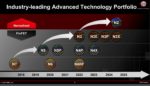
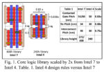
As I previously wrote about here, Intel is presenting their Intel 4 process at the VLSI Technology conference. Last Wednesday Bernhard Sell (Ben) from Intel gave the press a briefing on the process and provided us with early access to the paper (embargoed until Sunday 6/12).
“Intel 4 CMOS Technology Featuring Advanced FinFET Transistors… Read More
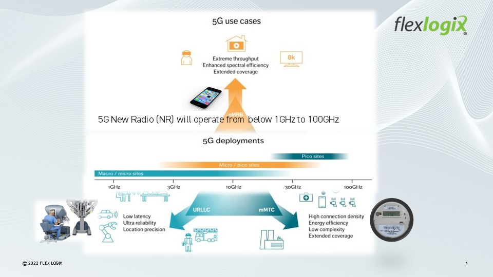
The demands of 5G requires new designs to not only save power but also increase performance and by moving to advance power-saving nodes and by using eFPGAs will help to achieve these goals. This paper will introduce 5G and O-RAN, the complexity of these systems, and how flexibility could be beneficial. Then we will dive into how eFPGA… Read More
From initial process technology development (TD) to high volume manufacturing (HVM) status for a new node, one of the key support functions to improve and maintain yield is the in-line wafer inspection technology. Actually, there are multiple inspection technologies commonly employed, with tradeoffs in pixel resolution,… Read More
There is no shortage of reporting on the many technological advances happening within the semiconductor industry. But sometimes it feels like we hear less in the area of semiconductor manufacturing equipment than in the design and product arenas. That doesn’t mean that there is less happening there or what is happening there … Read More


Musk’s Orbital Compute Vision: TERAFAB and the End of the Terrestrial Data Center