You are currently viewing SemiWiki as a guest which gives you limited access to the site. To view blog comments and experience other SemiWiki features you must be a registered member. Registration is fast, simple, and absolutely free so please,
join our community today!
WP_Term Object
(
    [term_id] => 50
    [name] => Events
    [slug] => events
    [term_group] => 0
    [term_taxonomy_id] => 50
    [taxonomy] => category
    [description] =>
    [parent] => 0
    [count] => 1522
    [filter] => raw
    [cat_ID] => 50
    [category_count] => 1522
    [category_description] =>
    [cat_name] => Events
    [category_nicename] => events
    [category_parent] => 0
    [is_post] =>
)
-SEMICON good conference -No news but perceptibly nervous
-Memory chip warnings & memories of cycles past haunt us
-Can we turn the clock back 20+ years on China Chip Policy?
-Last ditch efforts on Chips for America before government vacation
SEMICON West Conference
Attendance at the show was good, better than last Decembers… Read More
The VLSI Symposium on Technology and Circuits provides a deep dive on recent technical advances, as well as a view into the research efforts that will be transitioning to production in the near future. In a short course presentation at the Symposium, Marko Radosavljevic, from the Components Research group at Intel, provided … Read More
When I worked at EDA vendors and attended DAC, one of the most popular questions asked in the booth and suites was simply, “What’s new this year?” It’s a fair question, and yet many semiconductor professionals are so focused on their present project, using their familiar methodology, that they simply… Read More
Whether it is fully autonomous driving, or wrinkle-free fabric, or ambient energy harvesting for powering electronic devices, each industry is chasing after its respective ultimate goal. For the semiconductor design industry, its goal is the capability to generate complete chip or IP in executable format from a high-level… Read More
The Design Automation Conference has been the pinnacle for semiconductor design for almost 60 years. This year will be my 38th DAC and I can’t wait to see everyone again. One of the companies I will be spending time with this year is Altair.
Last month Altair acquired our friends at Concept Engineering, the leading provider… Read More
When more than one person is working on any project, coordination is imperative. When the team size grows, being in sync becomes essential. When it comes to SoC design management, registers and bit fields are used to communicate status of results and execute conditional controls. The Register Management function plays an essential… Read More
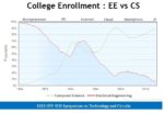
At the recent VLSI Symposium on Technology and Circuits, a panel discussion presented a jarring forecast. The theme of the panel was “Building the 2030 Workforce: How to Attract Great Students and What to Teach Them?”, with participants from academia and industry, as well as a packed (and vocal) audience.
On the one hand, the … Read More
Chip design verification has long been a key component of any design project developing silicon intended to go into manufacturing. As designs become more complex, so does the manufacturing risk, and the focus on thorough verification becomes ever more critical.
Another dimension of complexity coming into play and considered… Read More
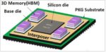
3D-ICs bring together multiple silicon dies into a single package that’s significantly larger and complex than traditional systems on a chip (SoCs). There’s no doubt these innovative designs are revolutionizing the semiconductor industry.
3D-ICs offer a variety of performance advantages over traditional SoCs. Because … Read More
Cadence Execs Look to the Futureby Dave Bursky on 07-01-2022 at 6:00 amCategories: Cadence, EDA, Events
Everything is becoming digital, and everything digital requires semiconductors. Cadence’s President and CEO, Dr. Anirudh Devgan, highlighted this at the recent CadenceLIVE user conference and discussed many of the company’s accomplishments and future directions. Dr. Devgan also sees the emergence of data—especially … Read More


Musk’s Orbital Compute Vision: TERAFAB and the End of the Terrestrial Data Center