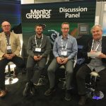
Mentor hosted a panel on emulation in their booth at DAC this year. One thing I really liked about this panel is that it didn’t include anyone from Mentor. Not that I have anything against Mentor employees, who are a fine bunch of people from those I know, but I find panels most interesting when the discussion is purely among customers.… Read More
Facebook and the Internet of Things
Something very important happened recently at the annual developer conference (F8). Facebook firmly staked its claim on IOT. Facebook events (like the Google annual developer events) are always interesting, as they give a tantalizing view of what is coming next. Yes, it lacks the panache the Apple events have. However, just … Read More
OpenPOWER Keeps On Truckin’ At Annual Development Summit
The OpenPOWER Foundation, a collection of companies that have coalesced around IBM’s POWER architecture recently had their OpenPOWER Summit in San Jose, California. OpenPOWER was founded by IBM, Google, Tyan and Mellanox to coalesce around IBM’s approach towards opening up the POWER architecture to anyone that wishes to license… Read More
Free Webinar: Designing Low-Power IoT Systems
As I have written before, IoT looks to be a key driver for design starts and future semiconductor revenue growth which is why we wrote “PROTOTYPICAL” and included a field guide to FPGA Prototyping. If you want to get funding for your new IoT chip project, having a working prototype is a good thing, absolutely. If you want to take a look… Read More
My #53DAC Must See List!
It may be hard to believe but this happens to be my thirty third Design Automation Conference. Where does the time go? Three of my kids are out of college and the last one is getting close. That is where my time has gone. The conference itself started in 1964 but my first one was in 1984 in Albuquerque, New Mexico. In fact, that was the year… Read More
A Shot in the ARM for IoT
I recently attended the IoT Developers Conference in Santa Clara, CA. There were clearly two major themes in the talks – security and low power. The volume market in IoT is in the edge node devices. These devices have two important characteristics. They acquire data which needs to be transmitted and they typically are battery-driven… Read More
Reusable HW/SW Interface for Portable Stimulus
Although semiconductor community has ushered into the era of SoCs, the verification of SoCs is still broken. There is no single methodology or engine to verify a complete SoC; this results in duplication of efforts and resources for test creation and verification at multiple stages in the SoC development, albeit with different… Read More
IMEC Technology Forum (ITF) – Moving the Electronics Industry Forward
IMEC is a technology research center located in Belgium that is one of the premier semiconductor research centers in the world today. The IMEC Technology Forum (ITF) is a two-day event attended by approximately 1,000 people to showcase the work done by IMEC and their partners.
Gary Patton is the Chief Technical Officer and Senior… Read More
Quick Guide to FD-SOI at #53DAC
If you’re headed to #53DAC (June 5-9 in Austin,TX) and are interested in learning more about FD-SOI, there will be lots of opportunities. Here’s a quick guide to get you started. … Read More


The Semiconductor Growth Numbers are Insane but the Real World Doesn’t Tally!