You are currently viewing SemiWiki as a guest which gives you limited access to the site. To view blog comments and experience other SemiWiki features you must be a registered member. Registration is fast, simple, and absolutely free so please,
join our community today!
WP_Term Object
(
    [term_id] => 50
    [name] => Events
    [slug] => events
    [term_group] => 0
    [term_taxonomy_id] => 50
    [taxonomy] => category
    [description] =>
    [parent] => 0
    [count] => 1553
    [filter] => raw
    [cat_ID] => 50
    [category_count] => 1553
    [category_description] =>
    [cat_name] => Events
    [category_nicename] => events
    [category_parent] => 0
    [is_post] =>
)
I’ve been attending DAC since the late 1980’s and can tell you that it’s an annual highlight for me and anyone else interested in the EDA, IP and semiconductor industries. Where else can you see most of the big and little vendors of EDA software, semiconductor IP and foundries in one place? I recently blogged about… Read More
At the SPIE Advanced Lithography conference I sat down with Mike Lercel, Director of Strategic Marketing for ASML for an update. ASML also presented several papers at the conference and I attended many of these. In this article, I will discuss my interview with Mike and summarize the ASML presentations.… Read More
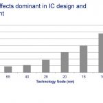
Designing an IC has both a logical and physical aspect to it, so while the logic in your next chip may be bug-free and meet the spec, how do you know if the physical layout will be reliable in terms of EM (electro-migration), IR (voltage drops) and thermal issues? EDA software once again comes to our rescue to perform the specific type… Read More
As feature sizes have shrunk, the semiconductor industry has moved from simple, single-exposure lithography solutions to increasingly complex resolution-enhancement techniques and multi-patterning. Where the design on a mask once matched the image that would be produced on the wafer, today the mask and resulting image … Read More
I’ve lived and worked in Silicon Valley for 13 years, but since 1995 I’ve been in the Silicon Rainforest (aka Oregon) where the world’s number one semiconductor company Intel, has a large presence, along with dozens of smaller high-tech firms. In the past year I’ve started to attend events organized … Read More
Much though some of us might wish otherwise, distributed development teams are here to stay. Modern SoC design requires strength and depth in expertise in too many domains to effectively source from one site; competitive multi-national businesses have learned they can very effectively leverage remote sites by building centers… Read More
Irresistible Materials (IM) is a spin-out of the University of Birmingham in the United Kingdom that has been doing research on Photoresist and Spin-On Carbon hard masks for 10 years, most recently with Nano-C on chemistry development. IM has developed a unique EUV photoresist and they are now looking for partners to help bring… Read More
TSMC Design Enablement Updateby Tom Dillinger on 04-10-2017 at 12:00 pmCategories: Events, Semiconductor, TSMC
A couple of recent semiwiki articles reviewed highlights of the annual TSMC Technical Symposium recently held in Santa Clara (links here, here, and here). One of the captivating sessions at every symposium is the status of the Design Enablement for emerging technologies, presented at this year’s event by Suk Lee, Senior… Read More
When thinking of ADAS from an embedded system perspective, it is tempting to imagine that system can be designed to some agreed margins without needing to worry too much about the details of the car environment and larger environment outside the car. But that’s no longer practical (or acceptable) for ADAS or autonomous systems.… Read More
Last week Intel held a manufacturing day where they revealed a lot of information about their 10nm process for the first time and information on competitor processes continues to slowly come out as well. I thought it would be useful to summarize what we know now, especially since some of what Intel announced was different than what… Read More


Consolidation and Competition: Who is Winning the $4.5 Billion Interface IP Race?