You are currently viewing SemiWiki as a guest which gives you limited access to the site. To view blog comments and experience other SemiWiki features you must be a registered member. Registration is fast, simple, and absolutely free so please,
join our community today!
            WP_Term Object
(
    [term_id] => 159
    [name] => Siemens EDA
    [slug] => siemens-eda
    [term_group] => 0
    [term_taxonomy_id] => 159
    [taxonomy] => category
    [description] =>
    [parent] => 157
    [count] => 835
    [filter] => raw
    [cat_ID] => 159
    [category_count] => 835
    [category_description] =>
    [cat_name] => Siemens EDA
    [category_nicename] => siemens-eda
    [category_parent] => 157
    [is_post] =>
)

WP_Term Object
(
    [term_id] => 159
    [name] => Siemens EDA
    [slug] => siemens-eda
    [term_group] => 0
    [term_taxonomy_id] => 159
    [taxonomy] => category
    [description] =>
    [parent] => 157
    [count] => 835
    [filter] => raw
    [cat_ID] => 159
    [category_count] => 835
    [category_description] =>
    [cat_name] => Siemens EDA
    [category_nicename] => siemens-eda
    [category_parent] => 157
    [is_post] =>
)
Test and Diagnosis at ISTFAby Beth Martin on 11-15-2012 at 7:10 pmCategories: EDA, Siemens EDA
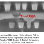
Finding and debugging failures on integrated circuits has become increasingly difficult. Two sessions at ISTFA (International Symposium for Testing and Failure Analysis) on Thursday address the current best practices and research directions of diagnosis.
The first was a tutorial this morning by Mentor Graphics luminary… Read More
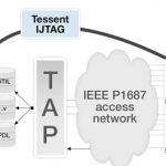
Until now, the integration and testing of IP blocks used in large SOCs has been a manual, time consuming design effort. A new standard called IEEE P1687 (or “IJTAG”) for IP plug-and-play integration is emerging to simplify these tasks. EDA tools are also emerging to support the new standard. Last week mentor announcedTessent IJTAG,… Read More
Test is the Rodney Dangerfield of EDA, it doesn’t get any respect. All designs need to be tested but somehow synthesis, routing, analog layout and the rest are the sexy areas. In my spoof all purpose EDA keynote address I even dissed it:You are short on time so slip in a quick mention of manufacturing test. Who knows anything … Read More
A Most Significant Manby Beth Martin on 11-06-2012 at 8:10 pmCategories: EDA, Siemens EDA
Most of us live perfectly good lives without distinction, fame, or note. Others rack up the honors, filling their walls and resumes with recognition of their brilliance. Like Dr. Janusz Rajski.
Rajski is the director of engineering for the test products at Mentor Graphics, an IEEE Fellow, and the inventor of embedded deterministic… Read More
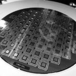
Our EDA industry loves three letter acronyms so credit the same industry for creating a five letter acronym CoWoS. Two weeks ago TSMC announced tape-out of their first CoWoS test chip integrating with JEDEC Wide I/O mobile DRAM interface, making me interested enough to read more about it. At the recent TSMC Open Innovation Platform… Read More
They say what adds value is to take something difficult and make it look simple. USB looks so simple when it is done right, but designers know it can be one of the more tempermental features in an SoC, especially in the latest SuperSpeed incarnation.… Read More
Mentor has a webinar on Model Driven Development (MDD) for Systems Engineering, presented by Bill Chown. It is actually the first of 15 webinars. This first one is just over 30 minutes long and I assume the others will be too. The webinar focuses on embedded system development, which historically has largely been validated using… Read More
Looking at the Press Release (PR) flow, it was interesting to see how TSMC has solved a communication dilemma. At first, let’s precise that #1 Silicon foundry has to work with each of the big three EDA companies. As a foundry, you don’t want to lose any customer, and then you support every major design flow. Choosing another strategy… Read More
My new iPad lasts about 10 hours on a single charge and the A5X processor is designed with a 45nm process from Samsung. Processor chips for tablets like this use a multi-voltage IC design flow to reduce total power by:… Read More
IC designers of passive devices often use empirical approaches to perform High Frequency Analysis (HFA), however there is at least one new approach being offered by Mentor Graphics using a tool flow of:
…
Read More