
Wyatt Earp probably wasn’t thinking of OPC when he said, “Fast is fine, but accuracy is everything,” but I’ll adopt that motto for this discussion of full-chip OPC and post-OPC verification models.
Accuracy is the difference between the calibrated model prediction and the calibration wafer result. Accuracy depends on several factors, principally the intrinsic ability to represent the patterning trends through target size, pitch, and pattern shape for 1D and 2D structures at a given process condition. Calibration test pattern design coverage is important whenever model accuracy is in question.
Additionally, because you judge OPC model prediction against experimental data, you must consider the experimental errors associated with the metrology data. For an ensemble of different test patterns, a model’s accuracy is limited by the experimental noise “floor.” Multiple repeat measurements (across wafer, across field) provide a better statistical representation and lower this noise contribution to the model. It is interesting to note that the standard error in the determination of the mean for typical OPC calibration structures is 0.5 nm for 1D and 1.5 nm for 2D.
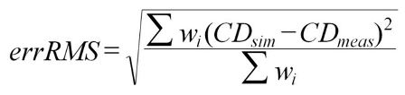
The degrees of freedom in the model will interact with the metrology noise such that it is possible to “over fit” the physical phenomena and start fitting the experimental noise.How can you quantitatively express the accuracy of a model? Metrics include maximum error, error range, chi-squared goodness of fit, and others. But one of the most useful is the “root mean square error value,” or errRMS (Equation 1) associated with the test pattern ensemble. This weighting (w) allows users to assign more importance to certain known critical design pitches. CDs may be used instead of EPE as well.
 [INDENT=2]Equation 1. CDsim[SUB]i[/SUB] is the model mean for each point i (measurement location); CDmeas[SUB]i[/SUB] is the data mean for each point i ; w is the user-specified weighting for each point i
An interesting variant of RMS error (see Schunn and Wallach 2005), which accounts for sample metrology error directly, is the scaled RMS deviation (Equation 2). This objective function more heavily penalizes errors associated with precisely known data points than for data points with CDs having larger uncertainties.
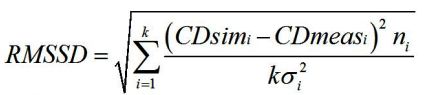 [INDENT=2]Equation 2. s[SUB]i[/SUB] is the standard deviation for each data mean i; n[SUB]i[/SUB] is the number of data values contributing to each measured mean; k is the number points i
A related, but ultimately more important characteristic is model predictability. The duty of the OPC or post-OPC verification model is to correctly predict the patterning for every possible layout configuration that can appear per the design rules in the full chip. The number of unique design constructs for low k[SUB]1[/SUB] lithography is tremendous; several orders of magnitude more than could ever be reasonably used to train the model. If you divide a master set of patterns into two sets–use one half to train the model, and the other half to verify–the errRMS fitness should be as low on both sets.
Another method involves including the complex 2D structures of the verification patterns, and then comparing the simulated contour with the experimental contour. If verification fitness is significantly worse than calibration fitness, the model is not sufficiently predictive. In addition, the model must account for CD variability arising from manufacturing process variability. Principle among these are focus, exposure, and mask CD variations (Figure 1).
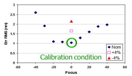 [INDENT=2] Figure 1. Example plot of model error RMS for various focus and exposure conditions. Model was calibrated at dose = Nom and focus = 0. Model fitness was then characterized for various defocus and exposure conditions.
As will be outlined in a future installment of this series, the ability of a model to faithfully predict various pattern failure modes is also important. These failures typically manifest more severely as these manufacturing process parameters vary. A final consideration related to predictability is model portability. Of course, if an entirely new photoresist material, PEB temperature, or etch recipe is implemented for manufacturing, you will need a new model calibration. But if some aspect of the exposure step is slightly altered, such as NA or illumination source intensity / polarization, you should be able to “port” the same resist model and change only specific optical parameters. This is particularly helpful in early process development, when an existing process model is used to simulate next node printing with whatever new RET capabilities may become available. The degree to which the model can decouple optical exposure from resist processing is related not only to the details of the resist model, but also to the nature of the approximations “upstream” in representing the mask and optical system. The details of these mask and optical models will be the topic of my next installment in this series of articles. Stay tuned.
–John Sturtevant, Mentor Graphics
P.S. In case you missed them, go readPart 1 and Part 2 of this series. Then continue with Part 4.
Share this post via:


Comments
There are no comments yet.
You must register or log in to view/post comments.