You are currently viewing SemiWiki as a guest which gives you limited access to the site. To view blog comments and experience other SemiWiki features you must be a registered member. Registration is fast, simple, and absolutely free so please,
join our community today!
WP_Term Object
(
    [term_id] => 157
    [name] => EDA
    [slug] => eda
    [term_group] => 0
    [term_taxonomy_id] => 157
    [taxonomy] => category
    [description] => Electronic Design Automation
    [parent] => 0
    [count] => 4438
    [filter] => raw
    [cat_ID] => 157
    [category_count] => 4438
    [category_description] => Electronic Design Automation
    [cat_name] => EDA
    [category_nicename] => eda
    [category_parent] => 0
    [is_post] =>
)
At #61DAC I stopped by the Defacto Technologies exhibit and talked with Chouki Aktouf, President and CEO, to find out what’s new in 2024. ARM and Defacto have a joint SoC design flow by using the Arm IP Explorer tool along with Defacto’s SoC compiler, which helps to quickly create your top-level RTL, IP-XACT and UPF files. This tool… Read More
An explosion in multiplier types/combinations lacking well-established C reference models for equivalence checking is prompting a closer look at theorem proving methods for verification. Paul Cunningham (GM, Verification at Cadence), Raúl Camposano (Silicon Catalyst, entrepreneur, former Synopsys CTO and now Silvaco… Read More
I stopped by the AMIQ EDA booth at DAC to get an update from Tom Anderson about their Integrated Development Environment (IDE), aimed at helping design and verification engineers save time. In my early IC design days we used either vi or emacs and were happy with having a somewhat smart text editor. With an IDE you get a whole new way … Read More
Dan is joined by Robert Ruiz, a product management director responsible for strategy and business growth of several verification products at Synopsys. Robert has held various marketing and technical positions for leading functional verification and test automation products at various companies including Synopsys, Novas… Read More
Babak A. Taheri, Ph.D., has served as Chief Executive Officer and member of the Silvaco board of directors from August 2019 to September 2021 and from November 2021 to present. From October 2018 to August 2019, Dr. Taheri served as our Chief Technology Officer and Executive Vice President of Products.
Tell us about your company?
…
Read More
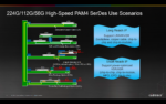
The rapid expansion of data-intensive applications, such as artificial intelligence (AI), high-performance computing (HPC), and 5G, necessitates connectivity solutions capable of handling massive amounts of data with high efficiency and reliability. The advent of 224G/112G Serializer/Deserializer (SerDes) technology,… Read More
I recall first blogging about Helix IPLM (formerly Methodics IPLM) at DAC in 2012, then Perforce acquired the company in July 2020, so I stopped by the Perforce booth this year at DAC to get an update from Martin Hall, Principal Solutions Engineer at Perforce. Martin’s background includes working at Dassault Systemes, Synchronicity,… Read More
#61DAC Is the place to go for the latest ideas, technology and products for semiconductor design and manufacturing. Between the exhibit floor and the technical program, you can get a vast education on almost any topic. In this post, I will focus on a unique company and a new version of a unique solution. IROC Technologies specializes… Read More
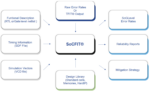
A Network-on-Chip (NoC) IP addresses the challenges of interconnect complexity in SoCs by significantly reducing wiring congestion and providing a scalable architecture. It allows for efficient communication among numerous initiators and targets with minimal latency and high speed. A NoC facilitates design changes, enabling… Read More
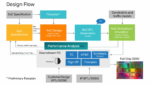
When I was at DAC last month, I had the chance to talk with Chouki Aktouf and Bastien Gratréaux from Defacto and they told me about a new innovative solution to generate Arm-based System-on-Chips. I heard that this solution has now been released.
Defacto and Arm developed a joint SoC design flow to help Arm users cover all needed automation—from… Read More


Chemical Origins of Environmental Modifications to MOR Lithographic Chemistry