Any doubters of the importance of FPGA technology to the defense/aerospace industry should consider this: each Airbus A380 has over 1000 Microsemi FPGAs on board. That is a staggering figure, especially considering the FAA doesn’t trust FPGAs, or the code that goes into them.… Read More
Electronic Design Automation
Jasper User Group Keynotes
I attended the Jasper User Group this week, at least the keynotes, the first by Kathryn Kranen the CEO of Jasper and the second by Bob Bentley of Intel.
Kathryn went over some history, going back to when the company was started (under the name Tempus Fugit) back in August 2002 with a single product for protocol verification. Now, since… Read More
Analog FastSPICE AMS — Simple, Fast, nm-Accurate Mixed-Signal Verification
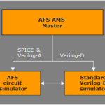
Verification and AMS are top search terms on SemiWiki so clearly designers have a pressing need for fast and accurate verification of today’s mixed-signal SoCs that include massive digital blocks and precision analog/RF circuits. They need simulation performance to verify the mixed-signal functionality, and they need nanometer… Read More
Cadence sets the Global Standards in VIP for AMBA based SoC
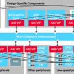
We have shown in Semiwiki how strong Cadence position was in Verification IP (VIP) in a previous post focusing on Interface standards like SuperSpeed USB or PCI Express. But IP based functions are used everywhere in a SoC, not only to interface with the external world, and need to be verified, as well, like for AMBA based functions.… Read More
Next Generation FPGA Prototyping
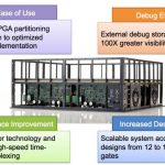
One technology that has quietly gone mainstream in semiconductor design is FPGA prototyping. That is, using an FPGA version of the design to run extensive verification. There are two approaches to doing this. The first way is simply to build an prototype board, buy some FPGAs from Xilinx or Altera and do everything yourself. The… Read More
Static Timing Analysis for Memory Characterization
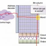
Modern SoC (System On Chip) designs contain a larger number of RAM (Random Access Memory) instances, so how do you know what the speed, timing and power are for any instance? There are a couple of approaches:
[LIST=1]
Carbon has Six Weeks of ARM, not to Mention Imagination and MIPS
As George E.P. Box said, “essentially all models are wrong but some are useful.” That is certainly the case with Carbon’s models. For processors they have two models, one that is fast (but not timing-accurate) and one that is accurate (but not fast). But both are useful.
Carbon attended the ARM TechCon in Santa… Read More
ICCAD at 30: Alberto Looks Back and Forward
At ICCAD earlier this week, CEDA sponsored a talk by Alberto Sangiovanni-Vincentelli looking back over the last 30 years (it is the 30th anniversary of ICCAD) and looking to the future. As is always the case in these sorts of presentations, the retrospective contained a lot more detail than the going forward part. Clayton Christensen… Read More
IJTAG, Testing Large SoCs
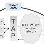
Test is the Rodney Dangerfield of EDA, it doesn’t get any respect. All designs need to be tested but somehow synthesis, routing, analog layout and the rest are the sexy areas. In my spoof all purpose EDA keynote address I even dissed it:You are short on time so slip in a quick mention of manufacturing test. Who knows anything … Read More
ARM adopting SpyGlass IP Kit, joining TSMC’s soft IP9000 Quality Assessment Program
More than one year old now, TSMC’s soft IP quality assessment program is a joint effort between TSMC and Atrenta to deploy a series of SpyGlass checks that create detailed reports of the completeness and robustness of soft IP. This soft IP quality program has been the first to be initiated by a Silicon foundry on other than “Hard IP”,… Read More


Siemens U2U 3D IC Design and Verification Panel